Used SEMILAB WT-2000PV #9181932 for sale
URL successfully copied!
Tap to zoom
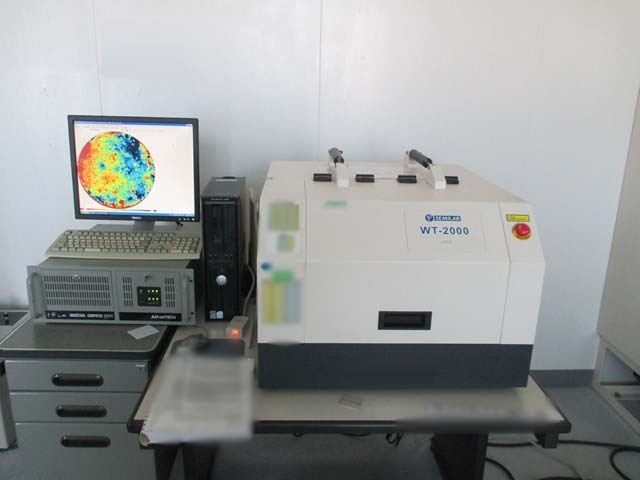


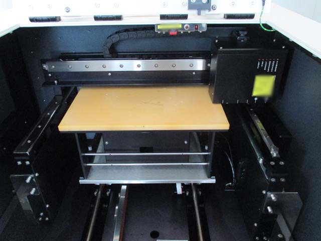

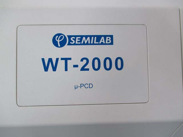

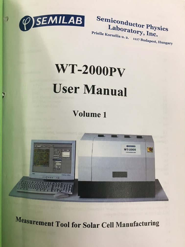

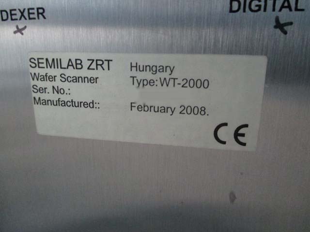

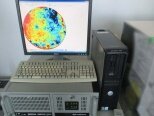
SEMILAB WT-2000PV is a top-of-the-line mask and wafer inspection equipment. This system is perfect for inspecting photomasks up to 32" x 32" in size with a maximum scanning area of 512 x 512 pixels and a maximum scanning speed of 8 cm2/sec. It is designed to meet the high-end demands of modern semiconductor fabrication and chip packaging applications, allowing users to identify and diagnose any faults as early as possible. SEMILAB WT 2000 PV is equipped with several advanced technological features for the most accurate visual inspection. Its fast DSP-based controllers provide both frequency- and amplitude-modulated scanning. It features a proprietary on-board PROBE software algorithm, a data acquisition unit, and a large-format LCD display with an intuitive, user-friendly graphical interface. The machine also has a dual laser beam tool for uniform illumination of the mask surfaces. This asset includes an automated defect recognition (ADR) feature to help users detect and address production defects quickly and accurately. ADR scans an entire mask or wafer and identifies patterns and other potential irregularities at high speed with high accuracy. It can also be used to identify production process failures and pinpoint their location. WT-2000PV also includes a high-quality CCD-based detector array. This allows users to accurately measure the amount of energy in the reflected light from each point on the surface of the mask or wafer. This feature is great for inspecting for any defects in the mask or for identifying materials such as gold, silver, and copper that may not be detectable with the help of the human eye. Furthermore, WT 2000 PV integrates all of the modern data output and communications needs of semiconductor fabrication and chip packaging applications. The model is compatible with a wide range of industry-standard protocols, such as Ethernet, USB, and RS-232. This allows users to easily share and store data, as well as transfer images, from SEMILAB WT-2000PV to other locations or devices. In short, SEMILAB WT 2000 PV is a highly advanced mask and wafer inspection equipment that is perfect for semiconductor fabrication and chip packaging applications. It features a range of advanced features to help users detect defects quickly and accurately, and its communication capabilities enable efficient data transfer and storage.
There are no reviews yet

