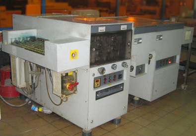
Used HOLLMULLER BAD-ADY / 65 #9016241 for sale
URL successfully copied!
Tap to zoom


HOLLMULLER BAD-ADY / 65 is an advanced photoresist equipment that is widely used in the semiconductor industry. It is composed of two main layers: the underlying (and often semi-permanent) photoresist layer, and the top "adiabatic" layer. The photoresist layer is composed of a polymeric material that is sensitive to light. When a pattern of light is exposed to this layer, the polymeric material will dissolve, leaving behind a pattern of holes in the photoresist layer that is only visible through the adiabatic layer. The adiabatic layer is composed of an epoxy-based material that is designed to ensure a uniform and continuous layer across the entire surface. It is this layer that provides the "protective" barrier against the underlying photoresist because it acts to reduce the amount of incident light that reaches the photoresist layer. This allows the pattern of holes to remain constant and predictable, no matter what variables are introduced to the system. BAD-ADY / 65 unit is ideal for semiconductor manufacturing because it allows high levels of precision and accuracy. It also has some degree of flexibility in terms of lightsource exposure, allowing for a wide range of exposure times to achieve different results. The machine has a surface passivation layer that helps to prevent any electrical charging effects from occurring on the finished product, thus increasing the yield of the product. The tool also has a post-exposure bake (PEB) process, which helps to harden the pattern created. This helps to reduce the shrinkage of the photoresist that is produced when light is exposed to it, preventing any inconstancies in the optical properties of the end product. Finally, it is also capable of achieving excellent imaging resolution, resulting in products with a high level of detail and clarity. Overall, the 1002HOLLMULLER HOLLMULLER BAD-ADY / 65 photoresist asset is a great choice for anyone looking to achieve high quality, precision, and accuracy with their semiconductor manufacturing process. Its uniform, adiabatic layer provides an effective and reliable barrier against incident light, while the PEB process and surface passivation layer provide further protection and accuracy. In addition to all of this, the versatility of the model allows for a wide range of exposure times, depending on the needs of the user.
There are no reviews yet