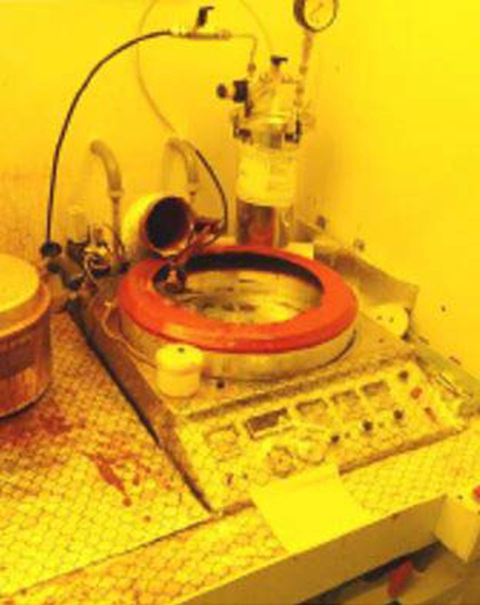
Used MITSUI SEIKI SP-40D #9230484 for sale
URL successfully copied!
Tap to zoom


MITSUI SEIKI SP-40D is a photoresist equipment designed for patterning semiconductor devices with high resolution. This system is equipped with an advanced microprocessor-controlled optical unit, a high resolution optics and advanced software for controlling the process of photoresist exposure. It is an ideal machine for patterning semiconductor substrates such as silicon wafers and other materials. The machine consists of an advanced optical tool, an illumination source, and a high precision scanning mechanism to provide an accurate mask to wafer registration. The illumination source can be an electron-gun or a high power LED source. The LED source is capable of providing higher resolution at a wider range of exposure conditions than an electron gun. The optical asset consists of a set of objectives and a motorized stage that allows for precise exposure alignments. The model is also equipped with an intuitive user-interface which enables easy parameter setting and process control. It provides process monitoring, data logging, process simulation, and data analysis for optimizing the process. The equipment also supports various types of software for controlling the photoresist exposure algorithms. SP-40D has a built-in auto-focus system which allows for automatic focus settings, making the process of photoresist exposure even simpler. In addition, this unit offers a wide range of processes such as spin-coating, etching, contact printing, wafer cutting, and pattern checking. It also provides options for varying process parameters such as illumination intensity, exposure time, scan speed, and post-exposure bake time. Overall, MITSUI SEIKI SP-40D is a powerful and reliable photoresist machine capable of providing accurate and high resolution photomasks for semiconductor device processes. It is designed to be user-friendly and offers a wide range of functions and features that can be easily configured according to the needs of each individual application. It can be used for a variety of patterning applications in the semiconductor industry.
There are no reviews yet