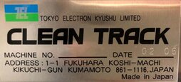
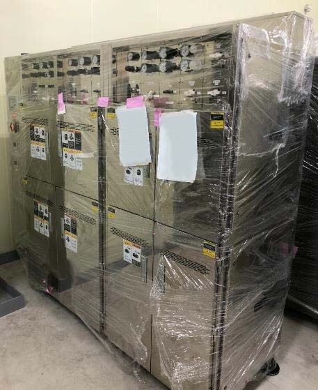
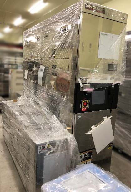
Used TEL / TOKYO ELECTRON Clean Track ACT 12 #9373073 for sale
URL successfully copied!
Tap to zoom





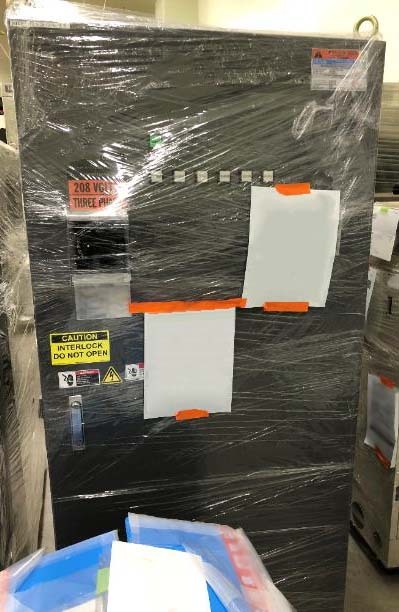

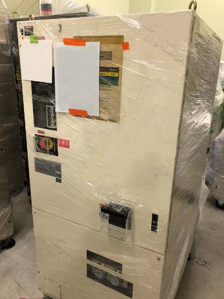

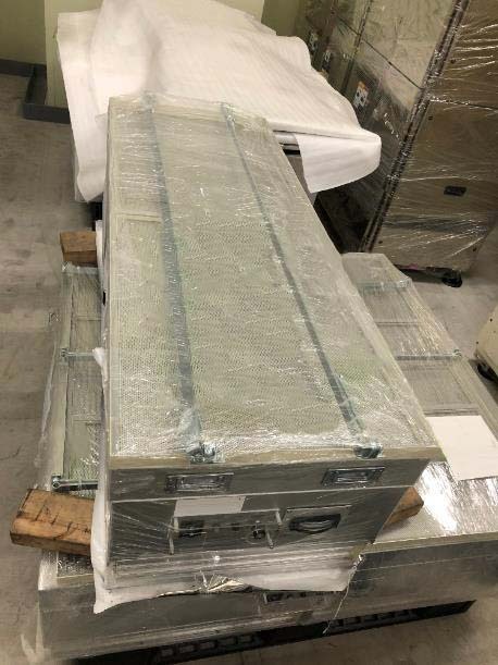

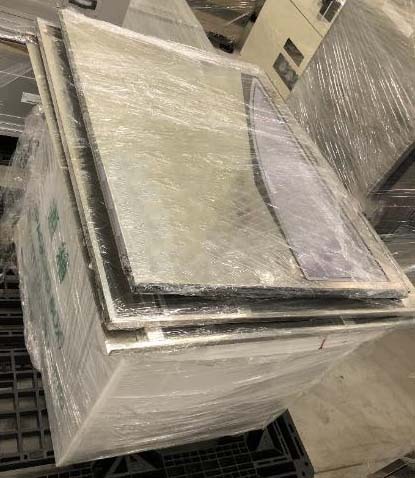


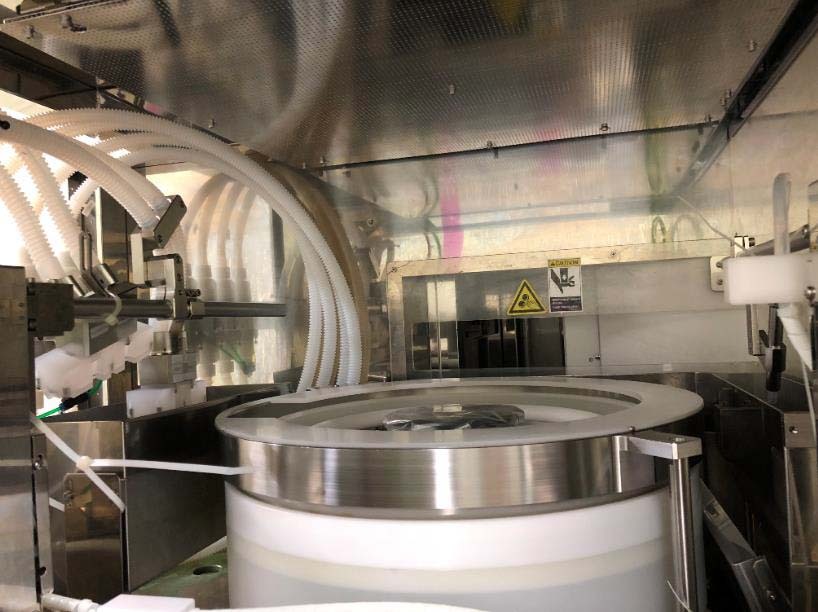


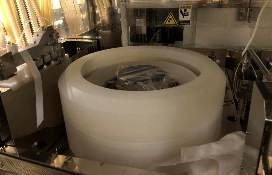

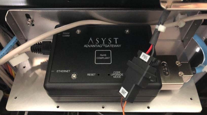


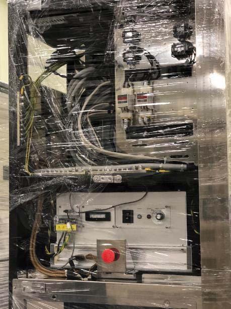


















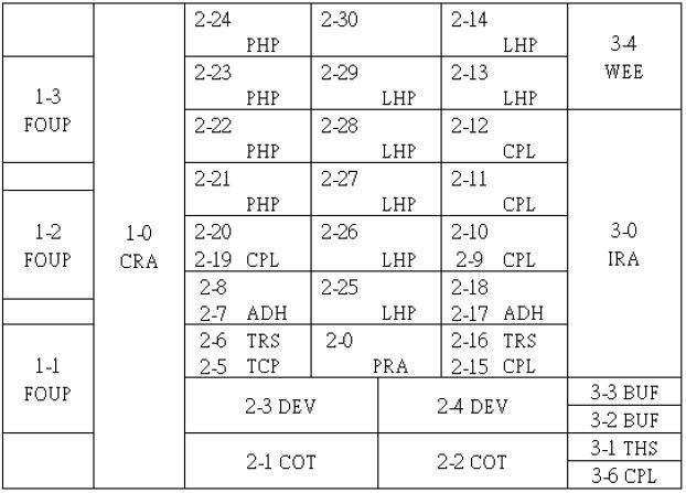


ID: 9373073
Wafer Size: 12"
Vintage: 2002
(2) Coater / (2) Developer system, 12"
Load port: (3) FOUPs
Main controller: Type 2
Coater 2-1 and 2-2:
R1-R4
(4) PR Nozzles
EBR
Resist pump type: RRC Pump
PR Filter type: Housing type
Developer 2-3 and 2-4:
Developing nozzle: Dual H nozzle
Top rinse: Single nozzle
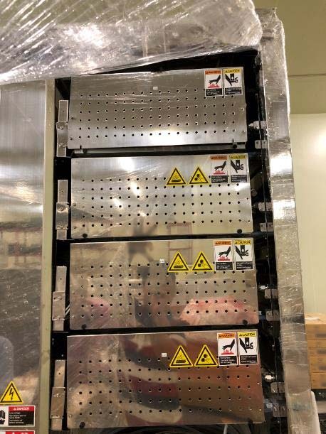
Plates: (2) ADH, (7) LHP, (5) CPL, (4) PHP, (2) TRS, TCP
IFB: WEE, Buffer, CPL, THS
SHINWA ESA-8-T-01 Temperature and humidity controller
SMC INR-244 Temperature control unit
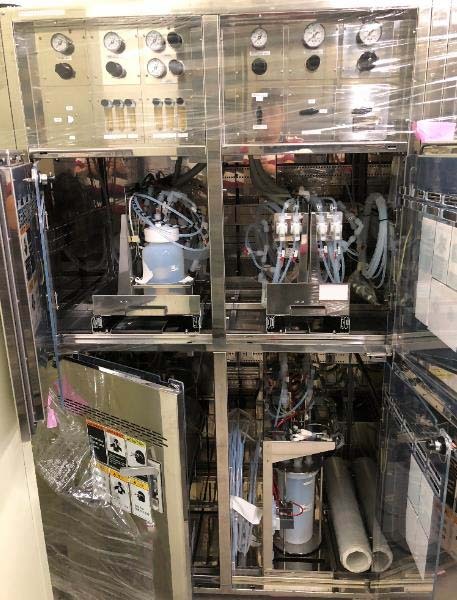
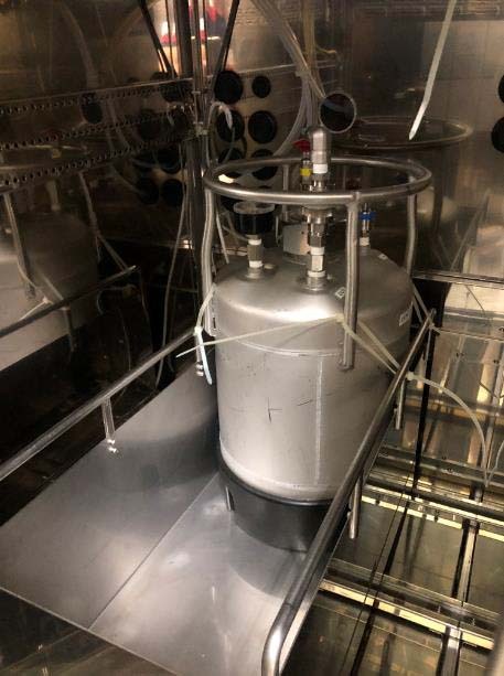
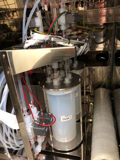
Chemical cabinet:
HDMS: Gallon bottle supply
Buffer tank: 3 L
Solvent: CSS With 3 L buffer tank
Developer: CSS with 3 L buffer tank
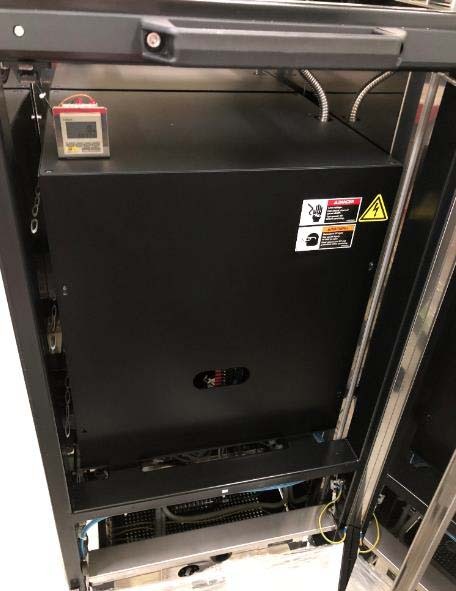
AC Power box: AC200/220 V, 157 A, 10 kA, 3 Phase
2002 vintage.
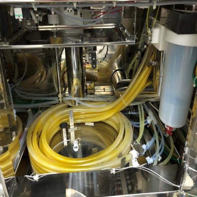
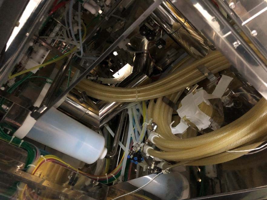
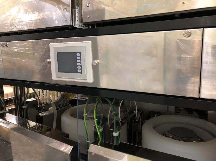
TEL / TOKYO ELECTRON Clean Track ACT 12 is a photoresist equipment designed to provide precision lithography on wafer imaging substrates. It enables advanced wafer processing techniques, including high throughput etching, high density contact exposure, and conformal coating applications. The system combines advanced particle control technology with robust hardware and software design for maximum lithographic yields. TEL Clean Track ACT 12 unit includes a 12-inch vacuum chuck with 6 multi-zone temperature control for rapid wafer processing. This is combined with an ultra-high vacuum process for wafer cooling, handling, and cleaning. This reduces the transfer of contaminants between exposed and unexposed regions of the wafer, ensuring that process results are consistent and interfere is minimized. The core of the machine is the CO2 laser-based projection lens that provides precise imaging and high aspect ratio exposure. The high-accuracy alignment tool delivers nanometer-level precision, offering the reliability and accuracy required for advanced lithography applications. The asset can accommodate up to 50 wafer size variations, including dual-sided exposure that doubles productivity by imaging both sides of the wafer simultaneously. Moreover, the extended focusing range of the model allows for 0.4 to 40-micron small line exposure, enabling users to reduce the production cost of circuits with medium to high density applications. The user-friendly process control software provides simple setup and simple operation, allowing for easy operation over a wide range of process recipes. The equipment is compatible with all major resists and developers, ensuring optimal photoresistance. In summary, TOKYO ELECTRON Clean Track ACT 12 system is a reliable and accurate photoresist unit designed to provide precise wafer imaging. Its robust hardware and software design, combined with advanced laser-based imaging and focus control, enable superior results for high throughput, small line imaging, and dual-sided exposure processes.
There are no reviews yet


