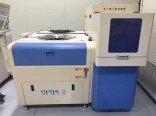
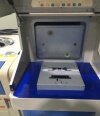
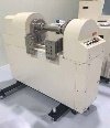
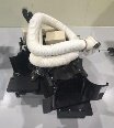
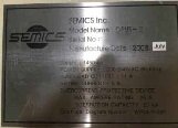
Used SEMICS Opus II #9134401 for sale
URL successfully copied!
Tap to zoom




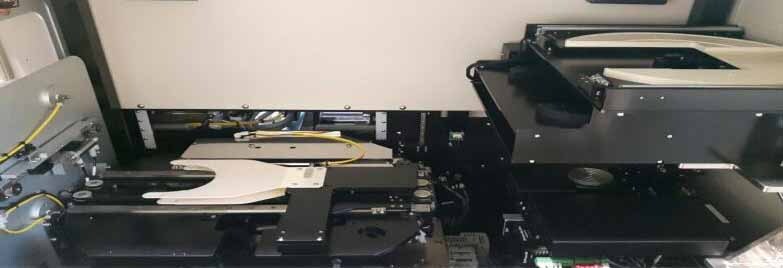


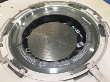

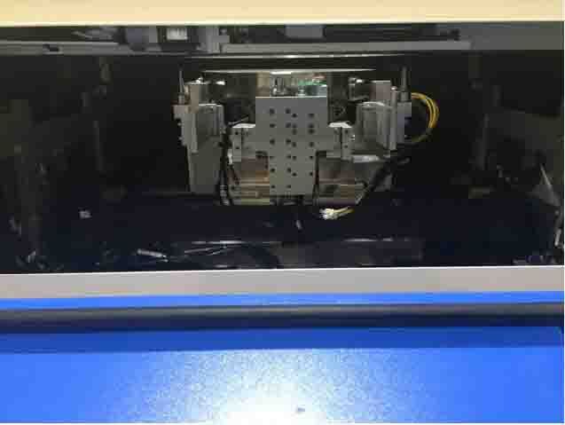

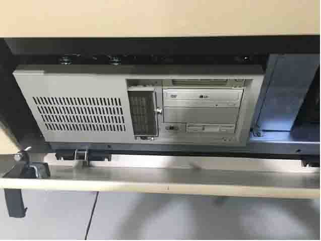




ID: 9134401
Wafer Size: 6"-12"
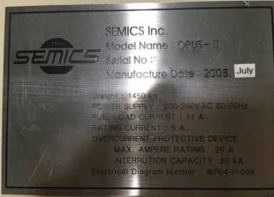
Vintage: 2008
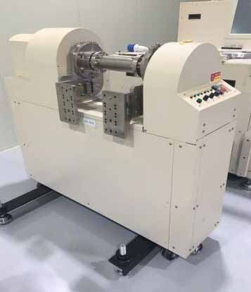
Prober, 12"
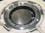
Chuck top: Nickel (Hot / Cold)
Cold option
Temperature: -55° C ~ 150° C
Cold temperature: -55°C
Air: Tube
Vacuum: Tube
Head plate
Monitor
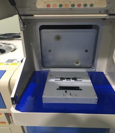
Needle cleaning unit: Square type
Manipulator
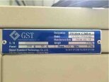
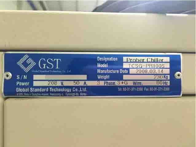
GST TCSG-PR100S Chiller
APC
Card holder
Hinge
Probe card changer
Docking with T5377S
Power: 200-240 V
2008 vintage.
SEMICS Opus II is a scanning electron microscope (SEM) prober designed for semiconductor inspection. It is capable of measuring electrical parameters such as threshold voltage, gate leakage current and channel carrier mobility, as well as measurements of small area surface topologies. The large size of the prober enables it to measure multiple devices on the same wafer simultaneously, while the precision and accuracy of the machine allow for precise measurements. Opus II consists of a vacuum envelope, a beam column and stage assembly, a probe station, and a specimen holder. The vacuum envelope serves as an environment where the specimen to be tested can be held in a vacuum. The beam column and stage assembly house the electron-optical components, namely the electron gun-source, electromagnetic lenses, and a target assembly. The probe station is designed to accurately mount and manipulate the probe to the specimen's surface. It also contains the necessary electronics for bias and electrical testing of the device under test. The specimen holder serves as a source of heat and is designed to hold up to four wafers at one time. SEMICS Opus II utilizes a field-emission scanning electron microscope (FE-SEM). This type of SEM utilizes an electron gun instead of a conventional thermionic source, which means that it is not limited by the effects of thermal energy. FE-SEMs are capable of providing detailed images of small surface topologies and also allow for electrical measurements of small devices. Opus II also offers various support functions that make it possible to accurately measure the devices under test. The sample surface can be automatically calibrated for precise placement of the probe on the device. It also allows for backside and frontside imaging, as well as electrical testing, to measure parameters such as threshold voltage, resistivity, and capacitance. SEMICS Opus II is an advanced prober designed to provide reliable and accurate test results for semiconductor devices. It is capable of measuring multiple devices on the same wafer and is able to provide detailed images of small surface topologies as well as precise electrical measurements. It is an effective tool for inspecting and testing the performance of semiconductor devices.
There are no reviews yet
