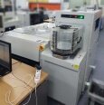
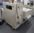
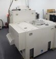
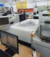
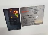
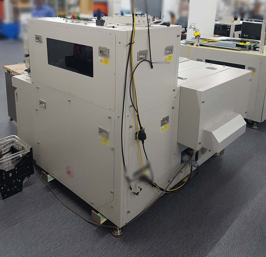
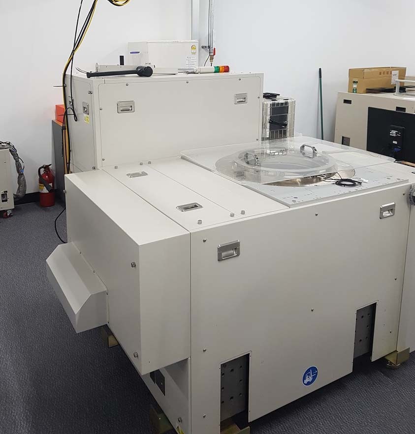
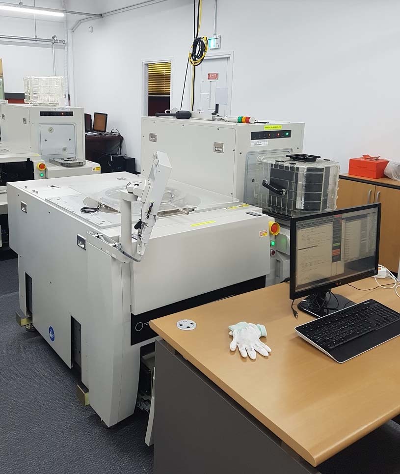
Used SEMICS OPUS III SL #9152235 for sale
URL successfully copied!
Tap to zoom





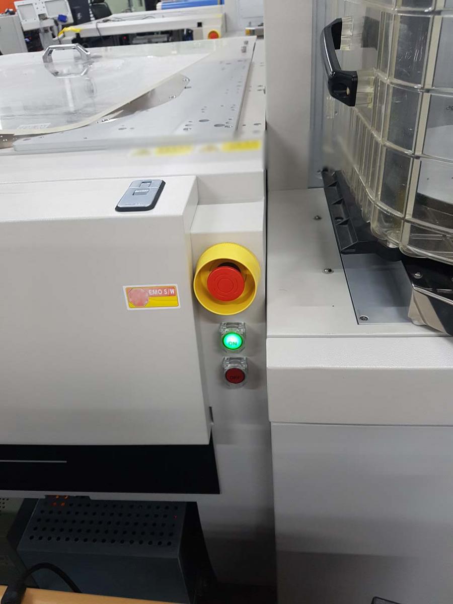


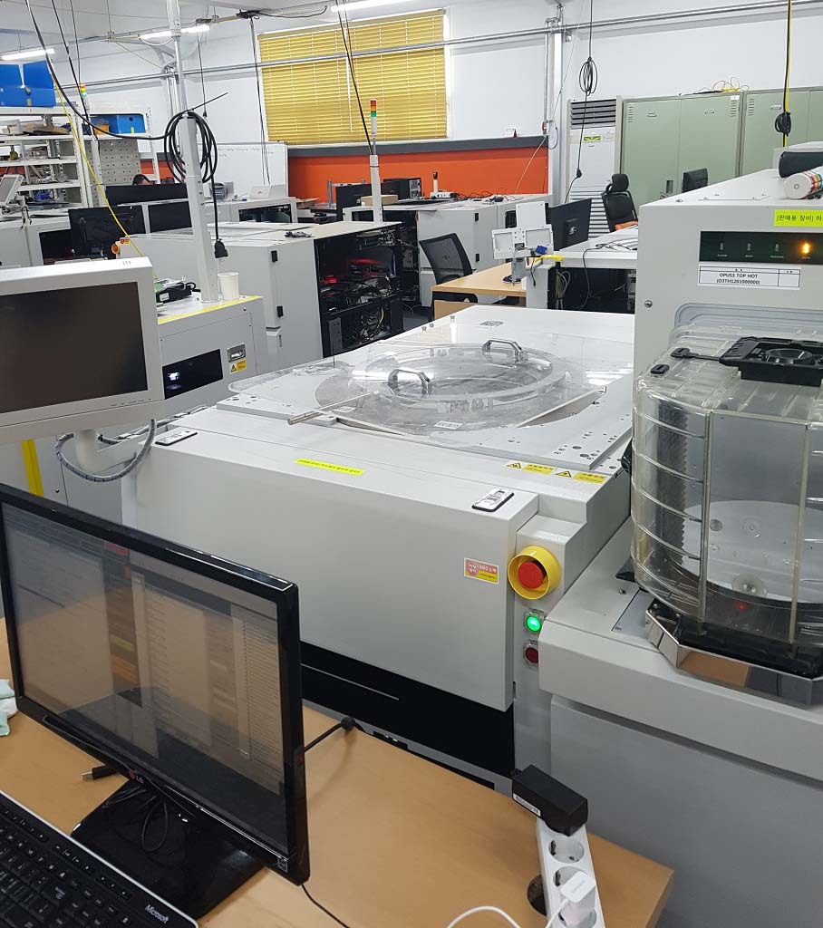


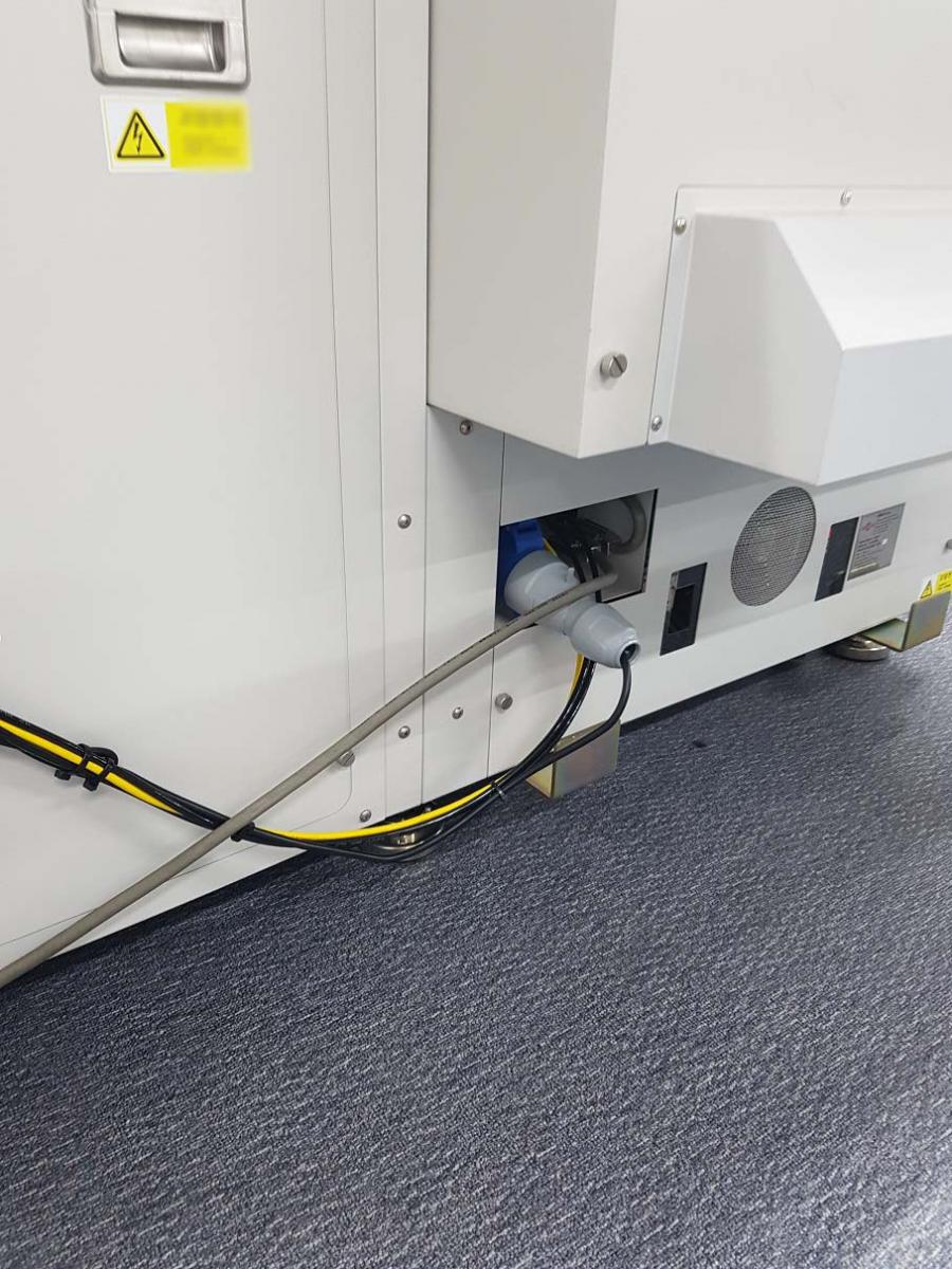

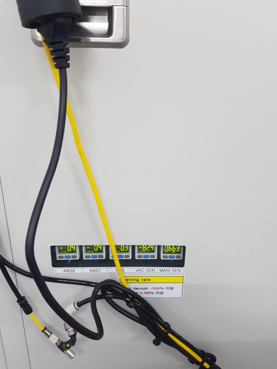

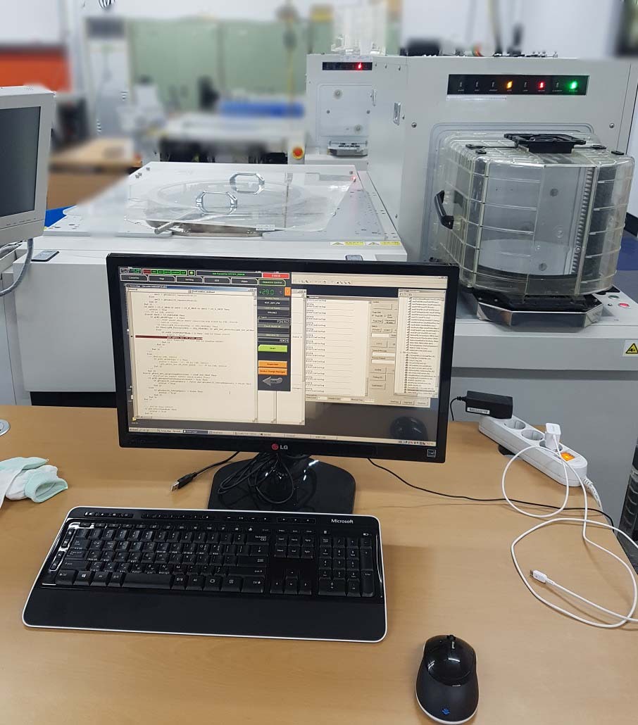

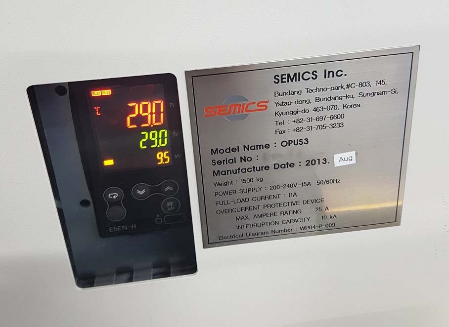

ID: 9152235
Wafer Size: 8"-12"
Vintage: 2013
Flat type hot prober, 8"-12"
First linear stage system
High accuracy / High performance
Cassette map with camera
GUI based on Windows
Soft contact: Low "K" device
Easy maintenance
VNC Support
Probe mark inspection
Main body:
System I/F: GPIB
Foup, 12"
Hot chuck, 12"
OCR Unit: SEMICS
Stage:
Card changer: Auto card changer: 350 mm
Head plate: Top head plate with auto tilt
Align camera:
Macro camera
Micro camera
Loader:
Arm: Arm 1, 2
Rotation unit: 360° Turn table
Elevator unit: 330 mm
Stroke AC servo motor
Wafer recognition unit: Camera
Fixed tray: Tray 1, 2
Inspection tray: Tray 1
Computer:
CPU: Pentium 4.2 GHz
Storage / Memory: 80 G HDD / 2G
Monitor: Touch screen, 15"
Operating system: Windows XP
Basic function:
PMI
PTPA
PTMA
PTPO
Needle polish
OCR
Manipulator:
Type: Hinge manipulator
Basic specification:
X, Y Stage:
Overall accuracy: ±1.5 μm
Probing area:
X: ±170 mm
Y: ±165 mm
Max speed: 300 mm/sec
Index time: 160 mm/sec / 10 mm
Resolution: 0.035 μm
Z Stage:
Withstand load: 300 kgf
Control accuracy: ±1 μm
Resolution: 0.18 μm
Full stroke: 30 mm
Speed: 50 mm/sec
Θ Axis:
Rotation range: ± 6º
Accuracy: ± 0.0002º
Resolution: 0.0025 μm
Chuck:
Planarity: 10 μm
Temp range: Ambient ~ +150°C
Temp accuracy: ≤ 100°C: 0.5°C
Air / Vacuum: External diameter tub: Φ 6 mm, 1 Line
Interface kit: ND3
Power:
Input power: 200~240 VAC
1 Phase (3 Wire)
Frequency: 50/60 Hz
Current: 25A
Air: 0.5 Mpa, 100 liter/min
Vacuum: -70Kpa ~ -100Kpa, 20 liter/min
2013 vintage.
SEMICS OPUS III SL is a prober specifically designed for testing interconnects on PCBs, MCMs, and ICs. It features highly accurate probing with its ultra-low mass, low-inertia probe head and features a unique multiple ratchet probe assembly for reliable and repeatable contact with your sample. It also has a custom-designed low-noise, low-temperature, low-vibration scanning stage for a more comprehensive probing solution. OPUS III SL is suited for a wide variety of applications including PCB testing, probing of individual components, surface mount assembly testing, wafer testing, IC package testing, and packaging inspection. The system features highly accurate probing for reliable and repeatable contact with your sample. The low-mass, low-inertia probe heads are designed for optimal probing short circuits and open circuits. The flexible scanning stage with a large X and Y travel range and multiple ratchet assemblies enable accurate, repeatable probing of your sample. The prober is designed to quickly scan large areas and features an user-friendly interface with intuitive graphical user interface and built-in scripting functions for automation. SEMICS OPUS III SL supports a wide range of electrical probing techniques, such as resistance measurements, capacitance measurements, current source-measurement, and power measurements. It also has system-level fault-tolerance functions such as contact bounce mitigation, low-temperature scanning and vibration compensation. The optional high-resolution camera enables fast, accurate, and repeatable optical inspections of your sample. OPUS III SL has configurable hardware, and can be upgraded to meet the specific needs of the customer. It also supports various customer accessories such as test fixtures, probe cards, adapters, benches, and more. It also has comprehensive mechanical and electrical safety systems for protection against short circuits, over-voltage and over-current conditions during testing. SEMICS OPUS III SL is an ideal tool for accomplishing a wide range of probing solutions. It is a highly-accurate, reliable, repeatable, and cost-effective prober for any quick or complex test set-up. With its wide variety of functionalities and user-friendly interface, OPUS III SL is the perfect prober for professionals looking to get the most out of their probing projects.
There are no reviews yet
