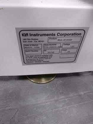
Used KLA / TENCOR 8100XP #9286582 for sale
URL successfully copied!
Tap to zoom
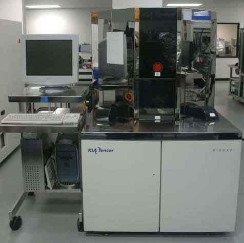

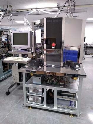

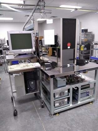

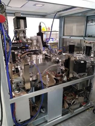

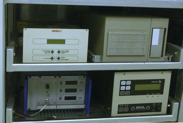






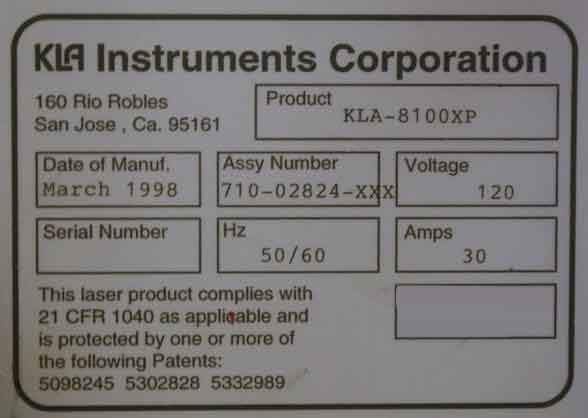

ID: 9286582
Vintage: 1998
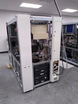
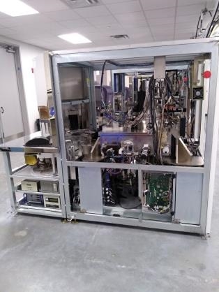
Critical Dimension Scanning Electron Microscope (CD-SEM), parts system
Computer
DELL Precision work station
Dual core processor
Raid array: (2) Drives
Operating system: Windows NT 4.0
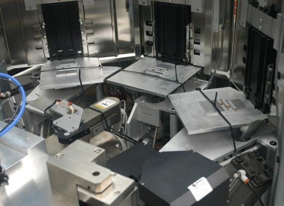
Cassette stations, 5"-8"
PRI Robot
With class 1 wafer scanner
Prealigner electron column
E Column electron source
Scintillator detector
Energy filter: (2) Wein filter apertures
1998 vintage.
KLA / TENCOR 8100XP scanning electron microscope (SEM) is the latest state of the art model, providing high-resolution imaging and precise analytical capabilities. This scanning electron microscope is ideal for a wide range of applications, from semiconductor failure analysis and sample examination to non-destructive testing with X-ray EDS. KLA 8100XP is an automated semiconductor defect inspection equipment. This system is capable of capturing high resolution images of samples at resolutions up to 0.5 micron. It uses both secondary electrons and instantaneous X-Y scan. Additionally, it can collect compositional and topographical data through its integrated Energy Dispersive Spectrometer. The unit features improved optics for low kV applications, providing superior image quality for a wide range of fields and applications. For materials analysis, TENCOR 8100 XP incorporates a combination of back-scattered electrons and secondary electrons that give an accurate representation of elemental composition. KLA / TENCOR 8100 XP is designed to increase productivity in the quality control process, providing information on flaw location, composition, size, shape, and geometry. It offers an easy-to-operate interface to quickly capture and analyze defects to make sure that product research and manufacturing processes attain the highest level of quality. TENCOR 8100XP is easy to operate. It is equipped with multiple automation features to quickly gather data and provide meaningful analysis without time-consuming manual adjustments. Additionally, advanced image analysis software can be used to compare data across multiple samples, in order to track the evolution and growth of individual defects. For basic material analysis, KLA 8100 XP can produce elemental line scans and spot analysis. This machine can also carry out higher level applications with automated drift correction and automated stages. 8100XP is incorporated with advanced filtration capability, allowing it to have a high level scanning stability for samples that are particularly sensitive to exposure to radiation. The integrated vacuum tool is designed to provide a clean environment for excellent imaging quality free from sample contamination or material buildup on the optics. 8100 XP's integration with KLA systems allows consecutive analysis of components and repairs, so that productivity can be optimized over extended periods. This asset is ideal for semiconductor failure analysis due to its advanced imaging capabilities, improved resolution, automated features, and user-friendly interface.
There are no reviews yet


