Used FISCHER Betascope #9246202 for sale
URL successfully copied!
Tap to zoom
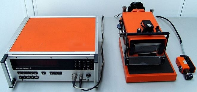

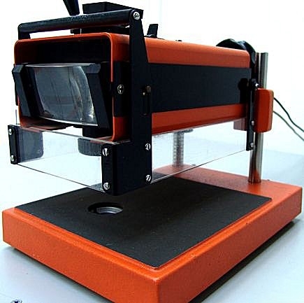

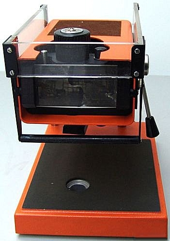


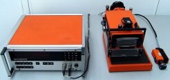
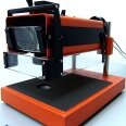
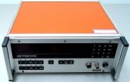
FISCHER Betascope is a wafer testing and metrology equipment from FISCHER Instruments. It is designed to measure and analyze a wide range of parameters associated with thin film and wafer metrology. It offers the advantage of a high-resolution optical interferometer and light detector with a median measurement accuracy of less than one nanometer. The system is capable of detecting a wide variety of features on the wafer surface, including layer thickness, surface planarity, feature geometry, and contaminants. The unit employs advanced algorithms to detect the shape and other features on the wafer surface. It also utilizes various illumination methods, such as dark field imaging, bright field imaging, contrast imaging, and optical probing. The machine includes a light diffraction unit, which is used to measure the interfering pattern from the incident light to measure the properties of the wafer surface. The tool includes image processing software for image enhancement and automated analysis, which can be done in real time. Betascope also offers a wide range of metrology options, including non-contact surface layer measurement, contactless shape analysis, non-contact numerical shape analysis, and advanced die-to-die surface feature measurements. The asset can also be used for the characterization of three-dimensional features on the wafer to improve yield. In addition, the model includes a powerful automatic visual inspection equipment to detect any defects or other surface anomalies on the wafer. The system also includes an automated wafer handling unit with an integrated robotic arm and gyroscope. This enables the machine to move to any point on the wafer automatically, providing precise and repeatable motion control when testing the properties of the sample. FISCHER Betascope tool provides a variety of options for data collection, storage, processing, and reporting. The asset's user interface is easy to use and can be customized to meet the specific needs of any customer. The data collected can be used in the analysis, optimization, and quality control of the wafer's physical properties and performance.
There are no reviews yet
