Used KLA / TENCOR Alpha Step 200 #293602539 for sale
URL successfully copied!
Tap to zoom
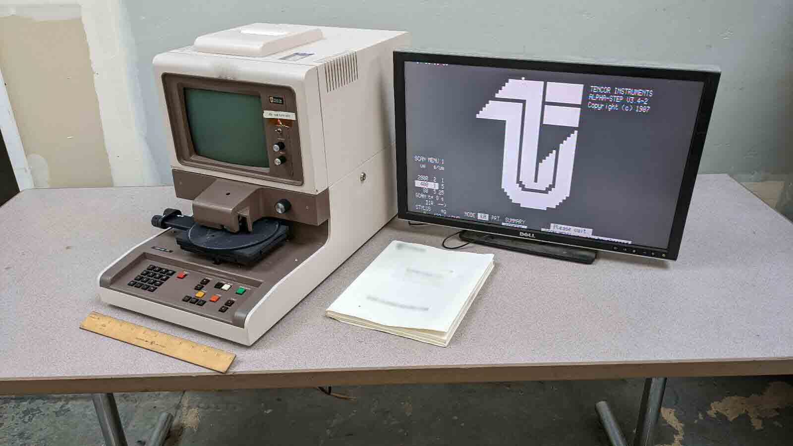

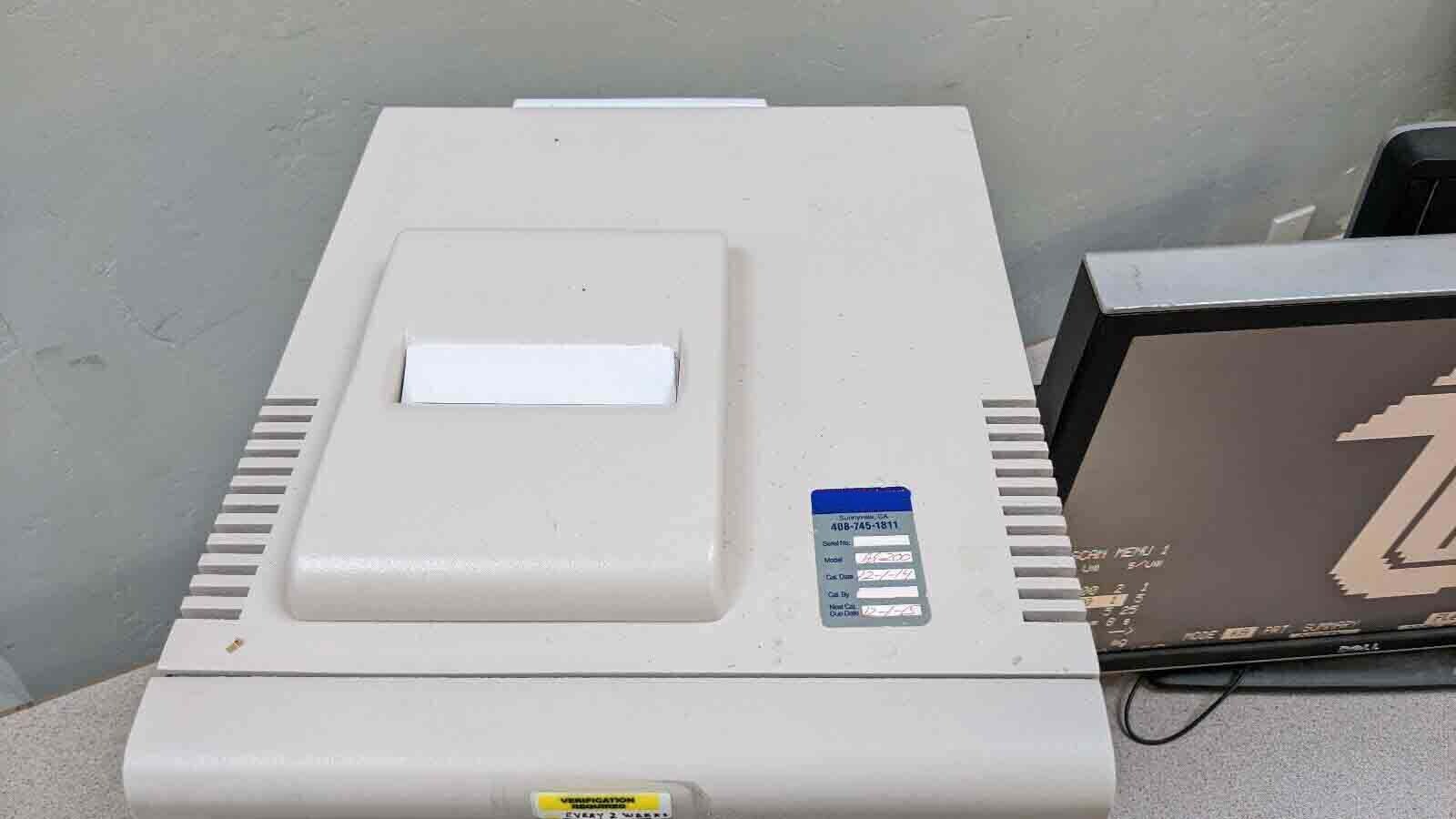

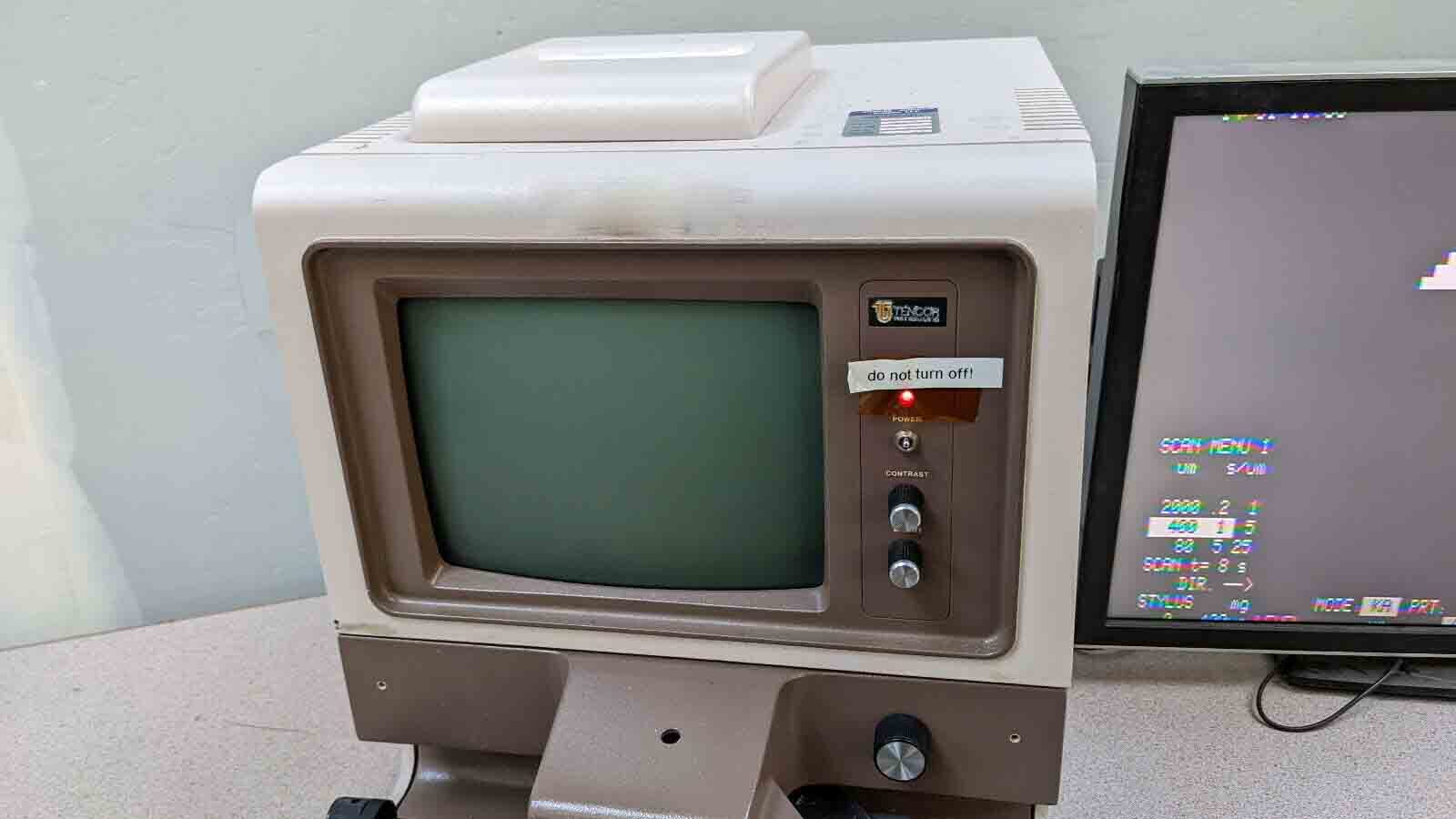

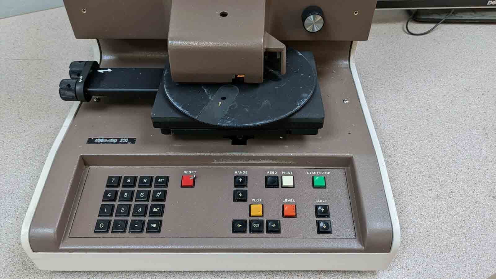


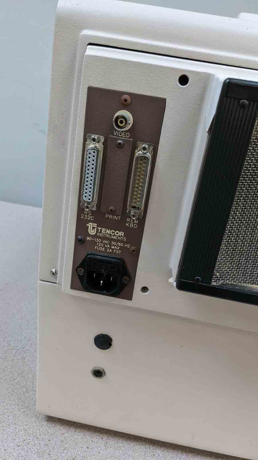

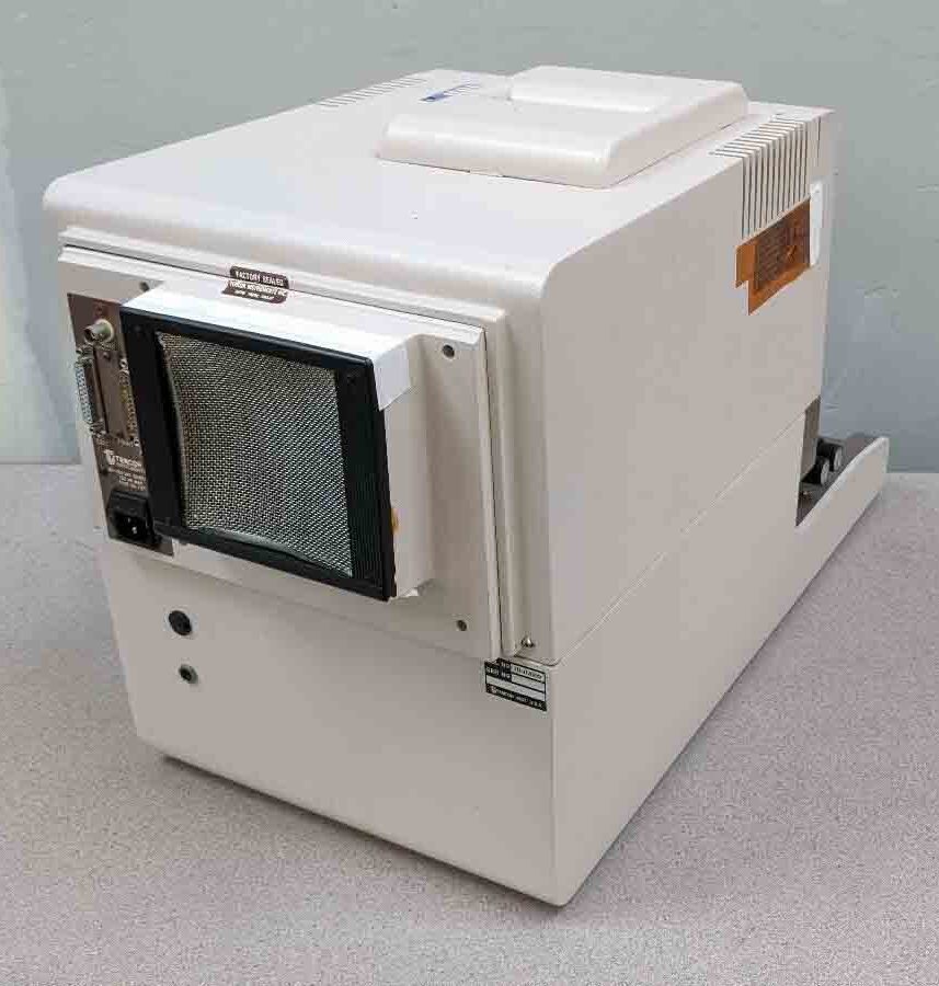

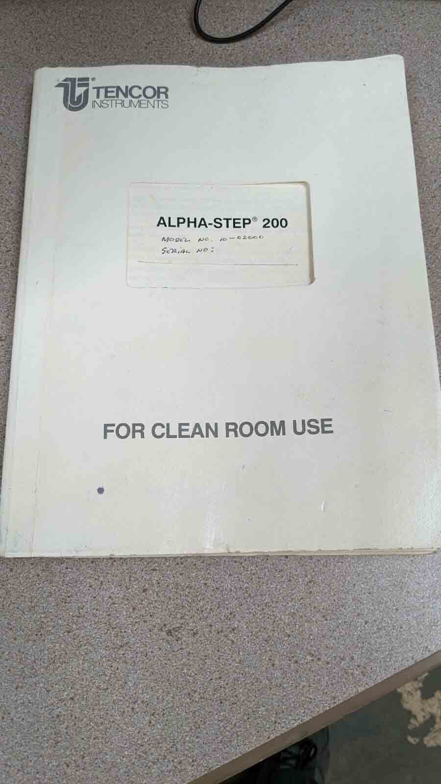


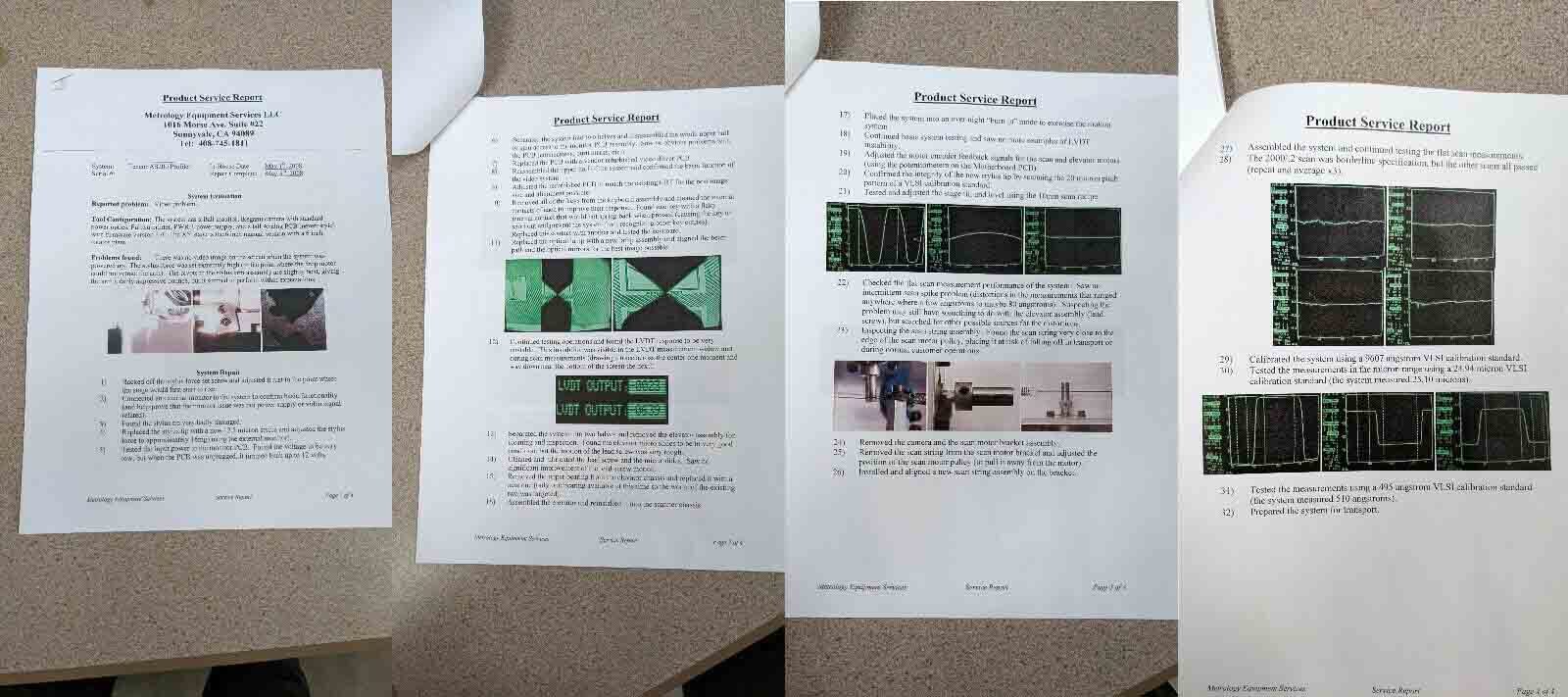

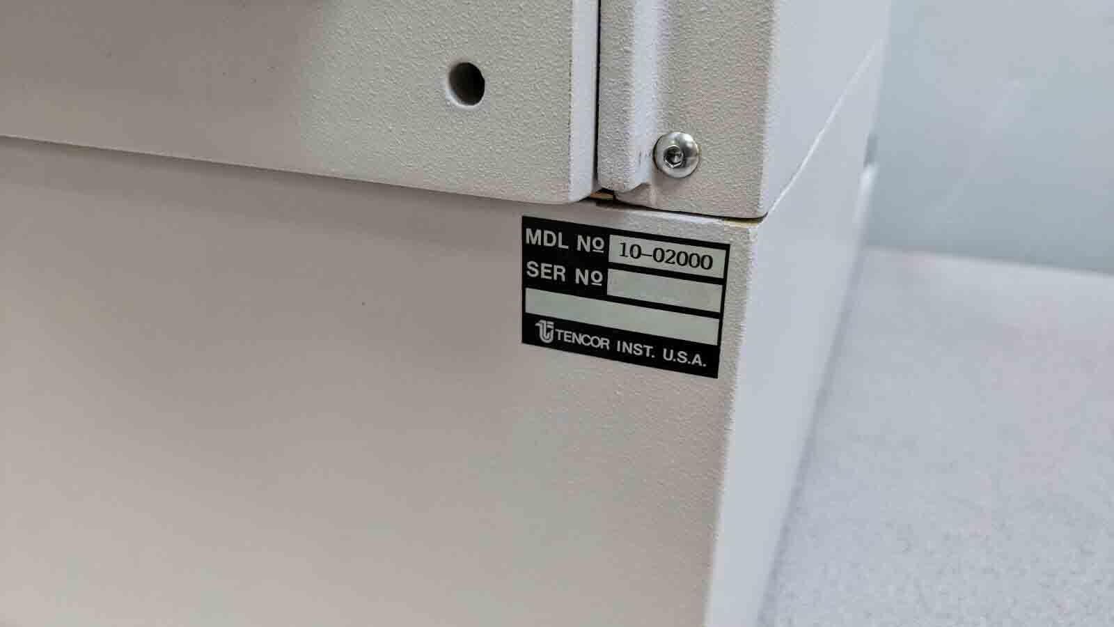

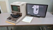
KLA / TENCOR Alpha Step 200 is a wafer testing and metrology equipment. It is used to measure the critical dimensions, roughness, and layer thickness of microelectronic and optoelectronic components. The system is capable of both optical and X-Ray analyses, and utilizes automated wafer mapping and comprehensive wafer defect analysis. Its Quantum (4D) optical reflectometer combines polarization, spectral and angle scanning to offer maximum flexibility and coverage. Its X-Ray unit uses an extendable two-axis gantry to collect high-resolution measurements quickly and accurately. KLA ALPHASTEP 200 is designed to decrease analysis time and associated costs by delivering information from multiple elemental collection methods. It can analyze a variety of wafer shapes, from circular to hard to access trapezoids, and is also able to collect critical multi-layer information with one run. Furthermore, its automated focus and zoom optically adjust to acquire data required to meet customer specifications. TENCOR ALPHA-STEP 200's Critical Dimension (CD) measurements can be done either optically or with X-Ray. The optical option uses a wide range of magnifications and variable directions of illumination, while the X-Ray option utilizes an extendable two-axis gantry structure that moves across the wafer surface dynamically. The X-Ray machine helps in achieving a precision of 2-10nm and can measure features down to 0.2µm. It can also resolve height differences of feature walls down to 5nm. KLA / TENCOR ALPHASTEP 200 is also capable of conducting in-situ Layer Thickness (LT) measurements. This feature is used to prevent layer cross-talk, discolorations, as well as other device reliability issues. Furthermore, its Roughness (R) map feature uses either the optically or X-Ray tool to measure mean peak-to-valley roughness on the wafer surface. Overall, ALPHA-STEP 200 is an advanced wafer testing and metrology asset for microelectronics and optoelectronics components. Its combination of optically and X-Ray analyses delivers an accurate and comprehensive range of capabilities. Its automated features and comprehensive defect analysis help to reduce costs and offer superior process understanding to enable high-quality, reliable products.
There are no reviews yet
