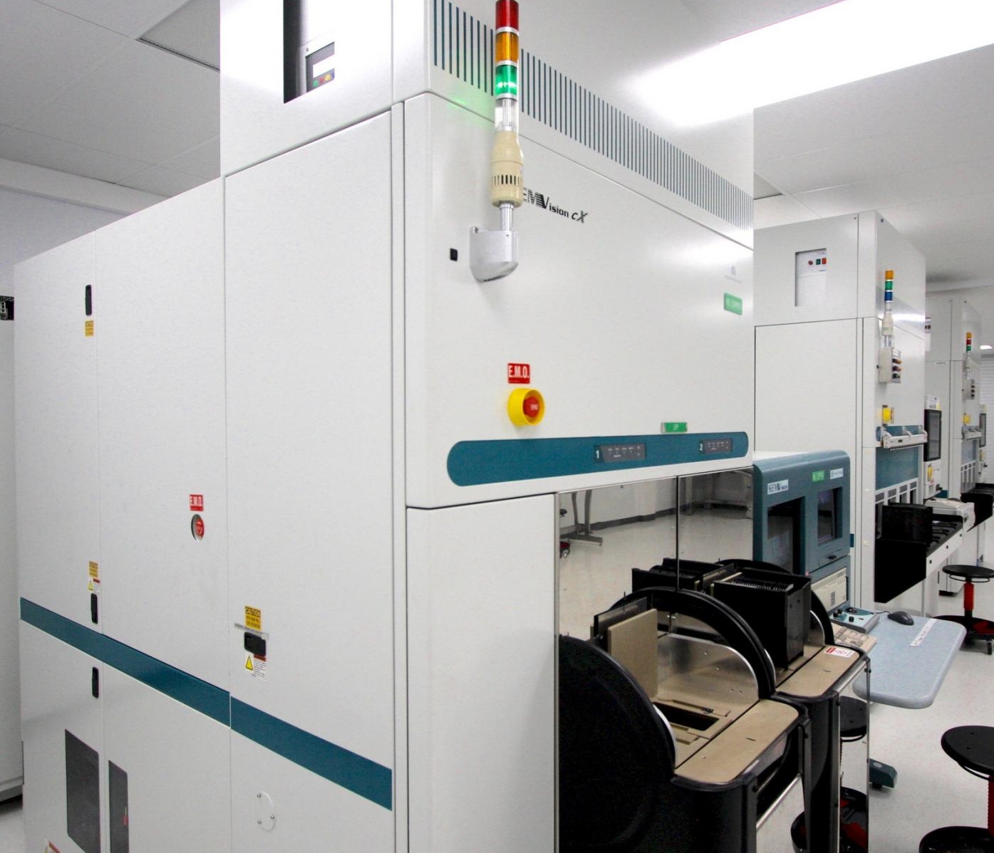
Used AMAT / APPLIED MATERIALS SemVision CX DR-300 #9159930 for sale
It looks like this item has already been sold. Check similar products below or contact us and our experienced team will find it for you.
Tap to zoom


Sold
ID: 9159930
Wafer Size: 8"-12"
Vintage: 2001
Automated defect review metrology system, 8"-12"
Wafer shape: Notch
Wafer handling:
Loader: SMIF / OCLP / AOD
FFU With ULPA filter
SEM / EDX Column
Tilt: 45 Deg column
Stage wafer holder 3 PIN
ETU 8" / 12"
ITU 8" / 12"
Aligner
Electron optical system:
Acceleration voltage: 150V - 15000V
Probe current: 10pA - 1.2nA
SEM Resolution: 4nm @1KV
Magnification: x200 - x200000
Maximum pixel: 1440
Multi perspective SEM imaging (MPSI)
VC Model (voltage contrast)
Optical microscope system:
Bright light / Dark field microscope
Objectives: 5x, 20x and 100x
SECS / GEM Communication interface:
Defect file format: Functionality confirmed to KLARF
Output file format: Same as input format
Host communication (SECS II / GEM /HSMS)
Wafer stage:
Stage accuracy: ±1.5um
Unique die-to-die
Single image automatic defect review (ADR)
Automatic defect classification (ADC)
Un-pattern review
Automatic process inspection (API)
E-Chuck stage: No (Pins stage)
Anti charge-3 (E-SEM)
Peripherals :
Port 1 / Port 2 type: OCLP
EDX
Tilt and rotation
Remote work station
Resolution target: Regular
Signal tower: Standard
EPDU
FIB: No
Facility:
Largest load ampere rating: 8 A
Full load current: 10 A
Interrupt current: 10,000 Amps I. C.
Supply voltage: 1-120 VAC, 1 Phase, 3-Wires
Power requirements: 208 V, 3 Phase, 5-Wires, 50/60 Hz
2001 vintage.
AMAT / APPLIED MATERIALS SemVision CX DR-300 is a mask and wafer inspection equipment designed to perform high-precision inspections of manufactured masks and wafers for semiconductor production. The system is capable of imaging and analyzing a range of wafer sizes and feature sizes, up to 8-inches (200 mm) in diameter. It is based on a unique Multi-Spectral Imaging (MSI) technology that provides unparalleled resolution and speed. AMAT SemVision CX DR-300 is a fully automated unit that is designed to quickly and accurately inspect semiconductor masks and wafers. It utilizes a patented Multi-Spectral Imaging technology that is capable of capturing high-resolution images of scanned wafers. This technology works by combining Light Emitting Diode (LED) and Organic Light Emitting Diode (OLED) illumination sources to produce an imaging pattern that is optimized for the specific application. The machine is also equipped with a variety of software and analysis tools for quickly and accurately detecting and identifying defects, including Phase-shift Defect Analysis and Defect Marking Capabilities. By combining the image capture and defect detection capabilities of the tool, it is able to quickly and accurately identify and report any defect or damage caused during the mask and wafer manufacturing process. Additionally, the asset is able to collect and store inspection results for future documentation and review. APPLIED MATERIALS SemVision CX DR-300 also features a variety of image navigation and inspection tools, providing users with the ability to easily locate, pan, zoom, and rotate images, as well as measure feature size and orientation. This ensures that all defects are quickly and accurately identified and documented. In addition, the model is also able to perform mask patterning inspections, allowing users to quickly and accurately measure the accuracy and tilt of the imaging pattern. Overall, SemVision CX DR-300 is a highly advanced mask and wafer inspection equipment. Its unique Multi-Spectral Imaging technology, combined with a suite of visualization and analysis tools, provides users with the ability to quickly and accurately identify and report defects in masks and wafers. In addition, its modular design allows it to be easily expanded to accommodate increased production needs.
There are no reviews yet