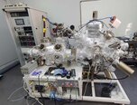
Used Molecular Beam Epitaxy for sale
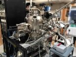
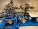
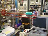
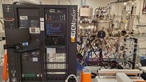
Molecular Beam Epitaxy (MBE) is a versatile and precise thin film growth technique used in the fields of materials science and semiconductor technology. It allows the deposition of high-quality epitaxial layers with atomic-level control over composition and thickness. MBE is commonly employed for the fabrication of structures and devices such as transistors, diodes, lasers, and photovoltaic cells. In MBE, the growth of thin films is achieved by molecular beams of elements or compounds ejected from individual effusion cells onto a heated substrate in a high vacuum chamber. The molecular beams consist of atoms or molecules that condense on the substrate surface, forming a crystalline layer with a well-defined crystal lattice orientation. The key advantage of MBE lies in its ability to grow epitaxial films with exceptional control, allowing the fabrication of complex multi-layered structures. The growth process can be precisely controlled by monitoring and adjusting the flux of the molecular beams and substrate temperature. This enables the precise control of film composition, thickness, and doping levels required for specific device applications. Additionally, MBE offers the advantage of low contamination levels due to the high vacuum environment. This results in high-purity films with excellent electrical and optical properties. The in-situ monitoring and characterization techniques available during the growth process further enhance the control and quality of the deposited films. MBE technology continues to advance with developments in strain engineering, lattice-matched growth, and the incorporation of novel materials. It plays a crucial role in the development of advanced semiconductor devices and is an essential tool for researchers and engineers working in the fields of materials science and nanotechnology.
Filters
-
(1)
-
(1)
-
(1)
-
(2)
-
(1)
-
(12)
-
(1)
-
(1)
-
(2)
-
(23)
-
(3)
-
(4)
-
(1)
-
(4)
-
(1)
-
(1)
-
(1)
-
(1)
-
(1)
-
(1)
-
(1)
-
(1)
-
(1)
-
(1)
-
(1)
-
(1)
-
(35)
