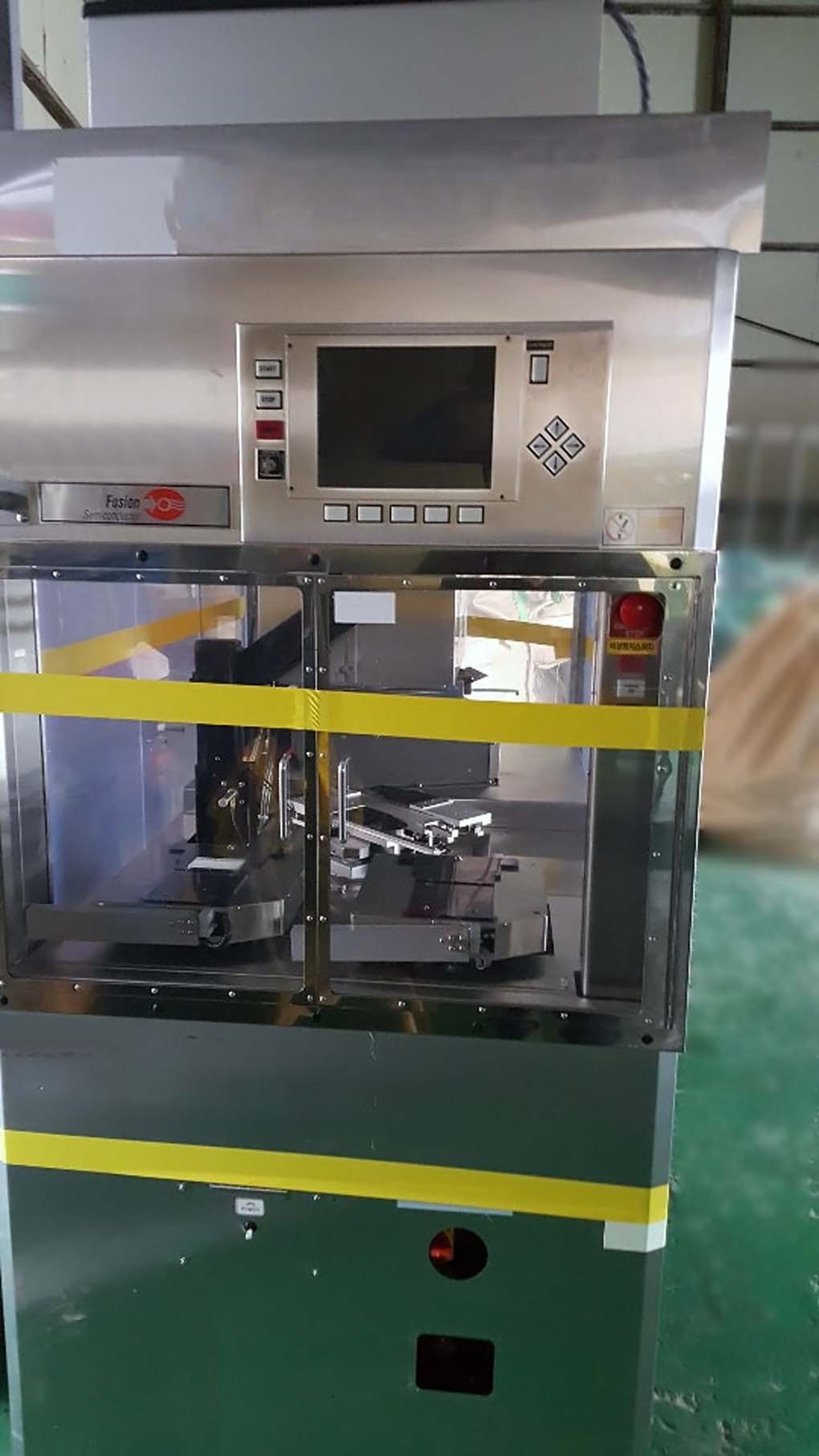
Used AXCELIS / FUSION M 200 PCU #9268836 for sale
It looks like this item has already been sold. Check similar products below or contact us and our experienced team will find it for you.
Tap to zoom


Sold
AXCELIS / FUSION M 200 PCU is an advanced exposure equipment designed for mask image writing in the semiconductor industry. The system provides fast and reliable image writing capability, excellent edge placement control, and superior throughput. With its precise laser control and excellent line-width accuracy, FUSION M200PCU enables manufacturers of semiconductor chips to meet their production needs. The unit is designed with a compact footprint and easy installation. The optical configuration consists of a high-power, high-speed UV laser source, a scanning head, an imaging optical machine, and a high resolution electron beam (EB) beam deflection tool. The scanning head utilizes a dual-axis deflection asset that allows very tight control over the beam delivery, resulting in reliable, precise, and repeatable imaging characteristics. AXCELIS M200 PCU provides changeable field size plates to allow varying exposure field times and different substrate sizes. It also allows for the integration of special features such as variable stage speed, uniform and non-uniform imaging fields, and flexible imaging field sizes. The laser source is designed to deliver high performance with low contamination and power consumption. The laser source utilizes an advanced Pulse Wave Modulated (PWM) model that ensures long-term reliability and stability. The laser source also incorporates a built-in cooling unit to minimize thermal degradation. The EB equipment is designed to provide excellent image repeatability and uniformity over an extended period of time. It features an improved electron source for higher electron beam power, and a high-resolution, high-precision deflector to provide precise control over image placement, making it well-suited for wafer patterning applications. AXCELIS / FUSION M200 PCU is designed to provide flexibility and superior performance for mask imaging and wafer patterning applications in the semiconductor industry. Its precise laser control, high-precision EB system, and advanced design features make it an excellent choice for meeting the needs of patterning and lithography process development.
There are no reviews yet