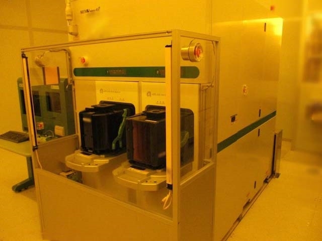
Used AMAT / APPLIED MATERIALS SemVision G2 #9190574 for sale
It looks like this item has already been sold. Check similar products below or contact us and our experienced team will find it for you.
Tap to zoom


Sold
AMAT / APPLIED MATERIALS SemVision G2 mask and wafer inspection equipment is the industry leader in high-precision lithography inspection, delivering superior image quality, accuracy and speed. The system offers an integrated image processing and inspection solution that is optimized for the most advanced lithography nodes, including 6nm and below. With the most advanced imaging unit, this type of inspection enables customers to guarantee the highest level of quality when it comes to product development. Using a dedicated imaging calibration for each feature size and node, this machine delivers the highest accuracy in visual die inspection as low as 6nm. With a bright, high-resolution 12" transmitted light imager and automatic focus, the tool provides sharp, clear images with reliable contrast across the entire image field. In addition to high-precision inspection, AMAT SemVision G2 also offers a non-destructive review of defects on masks and wafers with its patented automatic defect detection asset. This defect detection model is used to detect defects such as line-end bridging, pit bridging, line breakages, optical proximity defect (OPD) detection, particles and contamination. The equipment also offers an integrated scanning system that collects data from various devices such as CD measurement probe and FOUP. This unit can also be customized to perform CD slit or binary slit measurement, as well as aberration measurement. Furthermore, the machine allows customers to save valuable time in the development process by enabling fast, easy and accurate inspection and measurement. In terms of flexibility and productivity, APPLIED MATERIALS SemVision G2 tool offers a wide range of innovative features to meet customer's requirements. This asset offers the ability to reconfigure wafer dimensions on the fly and includes a novel load port architecture. It also comes with a user-friendly GUI interface, automatic tool selection and an intuitive, easy-to-use interface featuring simple navigation for complex operations. Overall, SemVision G2 model is the leading solution for mask and wafer inspection, offering advanced imaging and calibration for high-precision accuracy. Its integrated imaging and scanning offers accurate results with less time and money investment, allowing customers to be more efficient and productive in their process. With the highest quality images and the fastest defect detection, it offers the best in lithography performance for the most advanced lithography nodes.
There are no reviews yet