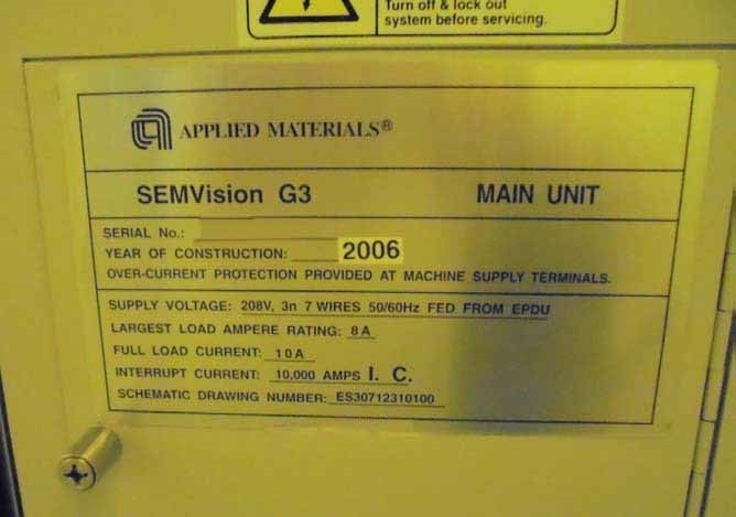
Used AMAT / APPLIED MATERIALS SemVision G3 #9261314 for sale
It looks like this item has already been sold. Check similar products below or contact us and our experienced team will find it for you.
Tap to zoom


Sold
ID: 9261314
Wafer Size: 12"
Vintage: 2006
Defect review system, 12"
Process: SEMREV
Wafer ID reader
Backside bar code wafer scribe reader
Carrier ID: Tiris compatable RFID
Operator access switch: VeritySEM-AUTO 8
Wafer mapping: Through beam mapper VeritySEM-AUTO 6
Optical FOV: Large optical FOV 100x, 20x and 2.5x
Tilt function
Contact hole profile grade
SECS Capable output VeritySEM-SYS2
Wafer stage: Anorad stage
Interlocks: ETU Access panel
Interface:
(2) FOUP (Continuous flow operation)
Remote units:
Dry and vacuum pumps
Signal tower: Red / Yellow / Green / Blue
Power supply: HVPS, CDM
Does not include dry pumps
CE Marked
2006 vintage.
AMAT/AMAT / APPLIED MATERIALS SemVision G3 is a new-generation mask and wafer inspection equipment designed to help chip manufacturers improve their process yields. It uses a suite of advanced machine vision technologies to accurately assess complex structures and layers of each mask and wafer, enabling faster and more reliable process control. The system provides detailed views of defects on a nanometer scale, helping accelerate and improve yield optimization efforts. AMAT SemVision G3 is equipped with an array of automated image and analysis capabilities. It employs high magnification optical systems for detailed pattern analysis, including the ability to inspect at the nano-level. It captures and reports defects, such as micro voids, bumps and scratches, on a range of materials including gallium arsenide and ferrite. This allows operators to accurately track and eliminate sources of errors quickly. The unit is built upon a comprehensive suite of hardware, software and data management tools. Its integrated sensors enable a variety of inspection methods, including dark field, bright field, oblique, off-axis and bright field assisted high-resolution imaging. To facilitate analysis and reporting, the machine is integrated with the latest in image processing and pattern recognition technologies, including 3D pattern detection, object classifications and flexible automated models. APPLIED MATERIALS SemVision G3 also offers a range of quality control and statistical process control services. These include defect detection, defect mask inspection and particle assessment. The tool also offers a range of failure analytics tools, providing operators with data-driven insights that enable informed decision making. In addition, SemVision G3 provides on-the-fly wafer matching and wafer grading services. These services use real-time scan data to assess patterns, identify anomalies and compare findings with expected performance. This helps manufacturers quickly assess and optimize the quality of their products. Overall, AMAT / APPLIED MATERIALS SemVision G3 provides an integrated, powerful mask and wafer inspection asset that helps chip manufacturers improve their process yields. Its advanced features, including pattern analysis, defect detection and analysis, wafer matching and grading, and failure analytics, make it a valuable tool for improving production quality.
There are no reviews yet