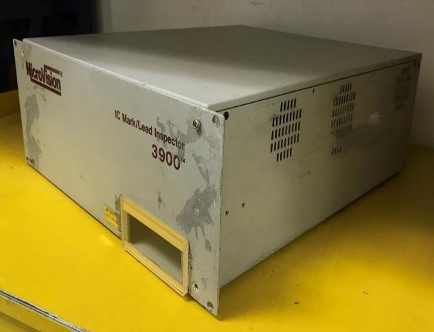
Used ESI / MICROVISION 3900 #9256529 for sale
It looks like this item has already been sold. Check similar products below or contact us and our experienced team will find it for you.
Tap to zoom


Sold
ESI / MICROVISION 3900 mask and wafer inspection equipment is a high-performance, intelligent, compact, and cost-effective solution for verifying mask and semiconductor wafer patterns. ESI 3900 provides comprehensive pattern inspection to ensure that wafer and mask patterns are within spec and free of defects. This system utilizes automated image acquisition, template matching, defect recognition, review, repair, and analytical functions to accurately and quickly inspect critical devices, such as embedded programmable logic devices (PLDs), memory systems, and flash cell arrays. With MICROVISION 3900, users can reduce wafer/mask development and acceptance costs, while boosting performance and reliability. 3900 includes a high-resolution projection unit and an automated major & minor defect detector. It can inspect 400mm wafers in just two minutes or less and offers optional particle cleanliness and die grouping. Its automated defect repair and propagation feature is capable of fixing minor defects in critical devices, thereby eliminating reticle and wafer processing failures. The machine incorporates a new generation of precise and advanced-performance alignment optics and an integrated charge-coupled device (CCD) line-scanned camera. It also features an optical image pattern recognition algorithm and defect control software that can detect all kinds of potential surface and mask defects, such as non-fill, misalignment, print-through, and more. The Microview ESI / MICROVISION 3900 is also compatible with multiple microelectronic fabrication processes, such as high-frequency (RF) processes, dielectric film, deep etch, and so on. This tool's design ensures ultra-low contribution to deformation artifacts, meaning that it can be used for wafer alignment and deformation control tasks with consistently high accuracy. Additionally, the asset offers powerful, user-friendly software that enables users to easily configure and control various parameters, from automated tuning for placement measurement accuracy to defect repair and propagation. The intuitive user interface also provides easy access to data review, navigation, comparison, annotation, and other processes. In summary, ESI 3900 mask and wafer inspection model offers an efficient solution for mask and wafer inspection. It combines a powerful set of advanced features, such as automated templates, defect recognition, repair, and propagation, with ease-of-use and accuracy.
There are no reviews yet