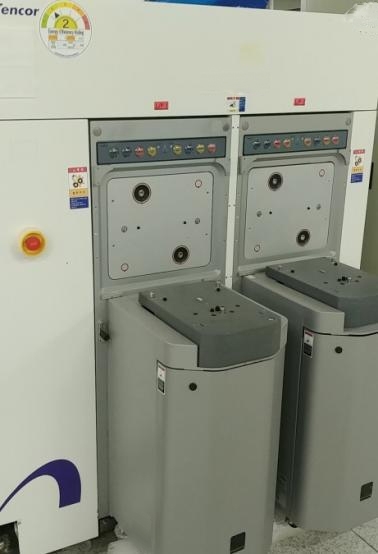
Used KLA / TENCOR 2350 #9270104 for sale
It looks like this item has already been sold. Check similar products below or contact us and our experienced team will find it for you.
Tap to zoom


Sold
ID: 9270104
Wafer Size: 8"-12"
Vintage: 2001
High-resolution imaging inspection system, 8"-12"
Dual open EFEM, 12"
GEM SECS and HSMS
Signal light towers: (4) Colors (R, Y, G, B)
Xenon lamp: 150 W
Wavelength illumination: 370~720 nm
Wavelength band: Visible, UV, I-line
Pixel size: 160~250 nm
User interface:
Monitor
Wafer display
Industrial PC (IPC)
Image computer (IMCs)
(44) IMC Boards
Does not include MM2S board
Inspection station:
Granite suspension: Power
Blower stage
Pneumatics optics plate
Air filter
Wafer handler (EFEM):
Dual open, 8"-12"
Dual SMIF, 8"
Dual FIMS, 8"-12"
Missing parts:
Hard Disk Drive (HDD)
Keyboard, mouse and joystick
Solenoid board
LP2 Cover
Robot controller
UI and IS connecting cable
RGB Cable
RS232 Cable
Joystick cable
EMO Cable
(4) IMACS to UI Cables
(2) AZP FFA Cables
MIB Cable
Digital camera cable
2001 vintage.
KLA / TENCOR 2350 is a Mask and Wafer Inspection Equipment designed to identify defects in semiconductor wafers and masks used in the production of advanced integrated circuits. This system utilizes a combination of illuminating and viewing functions, machine vision techniques, and image and data processing to detect and analyze defects that may otherwise be difficult to detect. KLA 2350 is equipped with an array of advanced optical components including a light source, a 5-megapixel CMOS image sensor, imaging optics, and specialized reflective and transmission optics. The unit's light source uses 6 narrow-band spectral slices in the visible and near-infrared (NIR) wavelengths to provide a high dynamic range and contrast for imaging both opaque and semi-transparent patterns. Additionally, the machine's imaging optics provide correction features such as field curvature and distortion, sharpness, lighting, and focus for improved tool performance. TENCOR 2350's CMOS image sensor is capable of scanning up to 10 wafers per second with a resolution of up to 500nm, ensuring high-quality image capture. The asset also offers wavelength-specific defect detections, which take advantage of the different illuminating and viewing functions to identify defects with specific wavelengths of light. To facilitate data analysis, 2350 features a powerful image and data processing model. This equipment is capable of measuring, analyzing, and classifying both mask and wafer defects. It is engineered with advanced algorithms to ensure the highest quality images and defect recognition, even in high-volume production environments. Additionally, the system is equipped with integrated inspection tools such as automated microscopy and image analysis software, which enable extremely precise and automated defect identification. KLA / TENCOR 2350 is a highly versatile and reliable mask and wafer inspection unit. With its advanced optics and powerful image processing and analysis capabilities, it has become an essential tool for the successful production of advanced semiconductor ICs.
There are no reviews yet