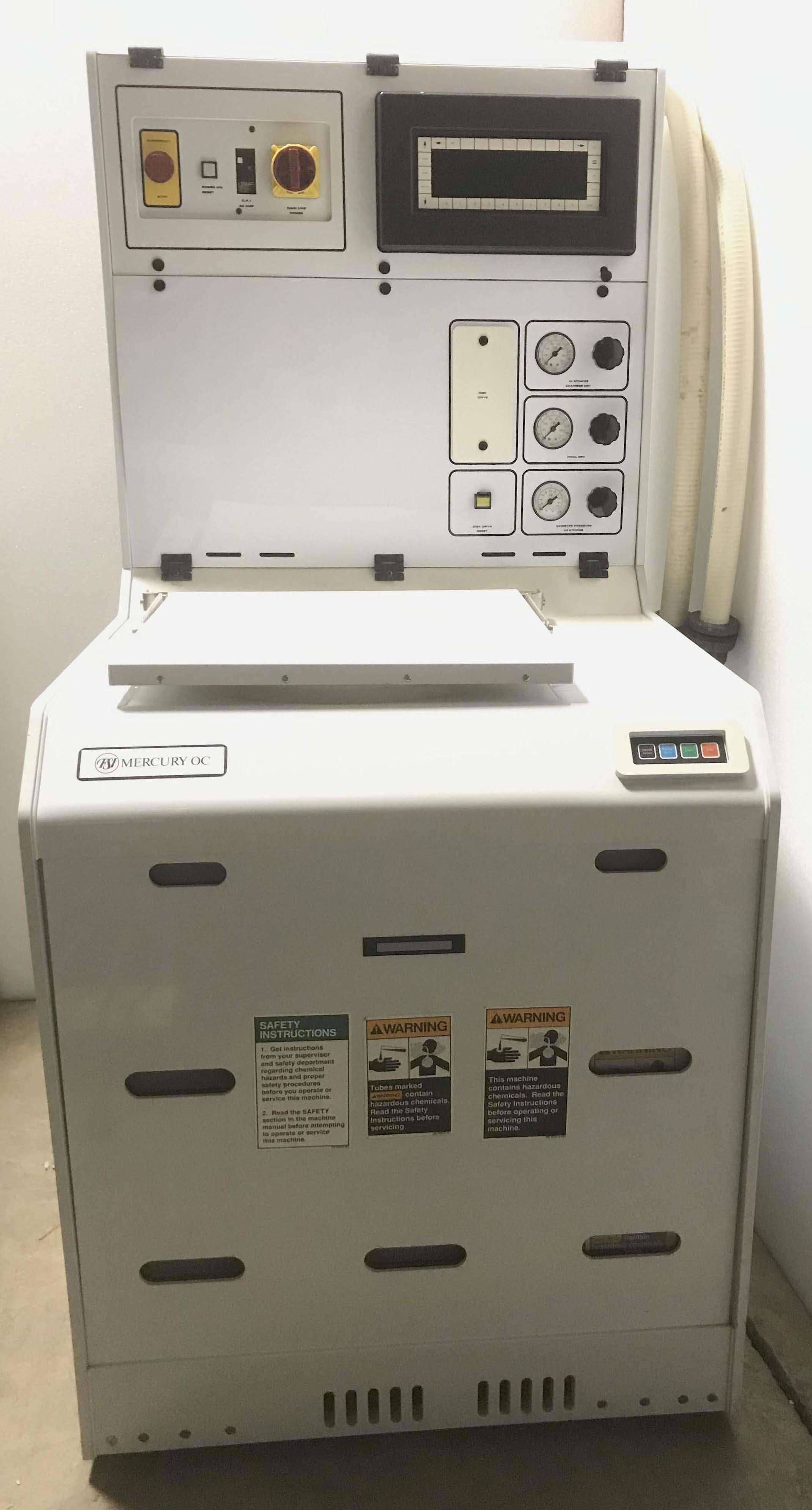
Used FSI / TEL / TOKYO ELECTRON Mercury OC #9233116 for sale
It looks like this item has already been sold. Check similar products below or contact us and our experienced team will find it for you.
Tap to zoom


Sold
ID: 9233116
Wafer Size: 5"
Spray processor, 5"
Single cassette, 8"
Diameter, 14"
A192-81M 25WH Rotor, 8"
Fed from central chemical distribution set up
No separate chemical carts with chemical canisters.
FSI / TEL / TOKYO ELECTRON Mercury OC is a photoresist equipment designed to provide highly accurate and repeatable imaging of the wafer surface. It is a single-column scanner featuring a stepper and scanner motion control system, which enables it to create highly accurate patterns on the wafer. The stepper and scanner motion control unit makes it possible to accurately position and eject the photoresist. The machine also features a high-resolution optical imaging tool and an integrated vision asset that allows it to quickly and accurately inspect its patterns for errors. The model is designed to work with a wide range of photoresist materials, including both positive and negative photoresists. It can produce images with resolutions of up to 0.1 micron, enabling it to produce extremely small and intricate patterns. The equipment also features an automated cleaning system that helps to keep the resist material clutter-free. This keeps the unit running at peak efficiency and ensures that patterns are produced consistently and accurately. In addition to its imaging capabilities, the machine offers other features designed to help streamline the wafer fabrication process. It has an integrated image sensor that enables it to register patterns on the wafer surface. It also features a patented "Auto Image Inspection" function that ensures consistent patterned results even at high-resolution levels. FSI Mercury OC is designed for use in advanced process technologies. It is suitable for use in semiconductor, MEMS and Nano-scale fabrication processes. It is ideal for prototyping and production of highly intricate structures with features as small as 0.1 micron. This tool is also suitable for use in creating next-generation electronic components, such as multi-level MEMS and NEMS structures. The asset is user-friendly and easy to operate, incorporating advanced motion control and image processing technologies. It is based on the latest computer software platforms, and is compatible with all common photoresist materials. The model also offers a long-term investment, with its long-lasting and reliable machinery making it the ideal choice for companies looking for an effective and cost-efficient solution to their wafer fabrication needs.
There are no reviews yet