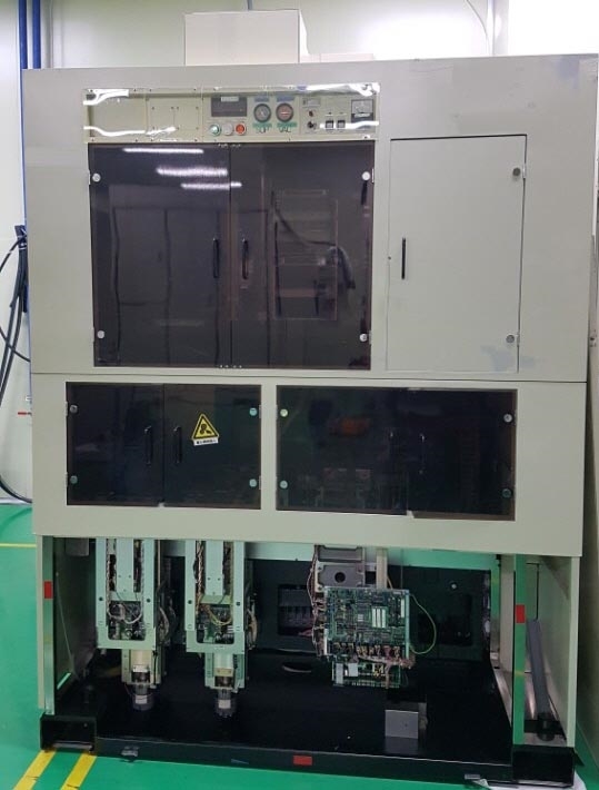
Used NIKON NSR 1755 i7A #9212123 for sale
It looks like this item has already been sold. Check similar products below or contact us and our experienced team will find it for you.
Tap to zoom


Sold
ID: 9212123
Wafer Size: 6"
Stepper, 6"
Chamber
Type: ASAHI S75
Set temperature: 24°C
FIA
PLC Type: MITSUBISHI MELSEC F1-60MR
Reticle microscope: 17.5 mm Variable
Reticle size: 5"
HP Laser:
5517 A
5 mW
ITV Camera: Custom
OF Detection type: NIKON
OF Sensor and OF ud motor: Normal 3.1:1
Wafer loader type: Type 1
Wafer condition: Silicon
Wafer carrier table: Right / Left
Rack type: Right
Does not include Electric source Nema box.
NIKON NSR 1755 i7A is a state-of-the-art production tool for photolithography. It is a high-precision wafer stepper that can produce advanced one- and two-level features as small as 0.025 µm in size. The equipment's integrated design combines high-throughput, processing power and stability for high-production volume manufacturing with extremely low yield loss. The nanometer overlay and registration accuracy ensures excellent line width control and uniformity across die. At the heart of the system is the high-accuracy six-axis motion robot, which maintains nanometer accuracy while providing a maximum acceleration of 6G. It is capable of trace-to-trace repeatability of less than 1nm. The robot is further integrated with a high-speed photo-mask changer and a high-precision substrate and mask aligner to minimize setup times. Other features of NIKON NSR 1755I7A include a variable, automated lens alignment unit, which accurately maintains alignment and focus quality, and a high-sensitivity, wide-range exposure machine with a dynamic range of 2 orders of magnitude. It is also scalable and upgradeable to meet future requirements. NSR-1755I7A is engineered for long cycle times and a wide range of substrates. It is designed to safely process between 55 and 253mm wafers and can operate at temperatures as low as 16°C to ensure minimum shrinkage at the edges. It is also capable of handling up to 30 exposures per wafer, reducing overall cycle times. The feature-rich NIKON NSR-1755 I 7 A makes it a preferred choice for many photolithography applications, including MEMS, optoelectronic devices, and semiconductors. Its advanced technology and high-performance capabilities make it an excellent choice for any size production, from prototyping to full-volume manufacturing.
There are no reviews yet