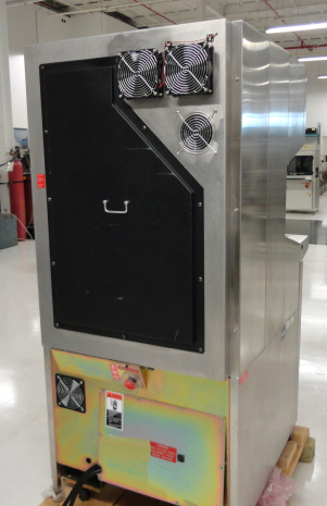
Used KLA / TENCOR 6220 Surfscan #181364 for sale
It looks like this item has already been sold. Check similar products below or contact us and our experienced team will find it for you.
Tap to zoom


Sold
ID: 181364
Vintage: 2001
Non-patterned Wafer Inspection System
Model No.: 519928
Compatible for 2", 3", 82mm, 4", 5", 6", 8"
Thickness: SEMI standard wafer thickness
Material: Any opaque, polished surface which scatters less than 5 percent of incident light
Smaller sizes factory-set at time of order
Defect Sensitivity: 0.09 micrometer diameter PSL sphere equivalent with greater than 80 percent capture rate
Haze/Sensitivity: 0.02 ppm minimum
Resolution: 0.002 ppm
Repeatability: Count repeatability error less than 0.5 percent at 1 standard deviation (Mean count greater than 500, 0.364mm dia. latex spheres)
Count Accuracy: Better than 99 percent (verified with VLSI Standards’ Relative Standard)
Spatial Resolution: 50mm spacing, minimum
Dynamic Range: 0.07 micrometer to 9,999mm in a single measurement
Throughput: 100 wph (200mm) at 0.12mm
Contamination: Less than 0.005 particles/cm2 greater than 0.15 mm dia. per single pass
Cassette Handling: Single puck wafer handling from two cassettes (one sender/receiver, one receiver)
Illumination Source: 30 mW Argon-Ion laser, 488 nm wavelength
Operator Interface: Mouse and/or dedicated user keypad
Physical Characteristics/Height: 168 cm (66 in.)
Shipping Weight: 300 kg (670 lbs)
Installation Requirements/Vacuum: 508mm (20 in.) Hg.
Electrical: 200-240V, 50/60 Hz
Power Requirement: 2 kVA
Ducted Venting: Two 102mm (4 in.) exhaust hoses
Environment: Class 10 or better
2001 vintage.
KLA / TENCOR 6220 Surfscan is a wafer testing and metrology equipment that can be used for a range of wafer level measurements. It is based on KLA optical wafer inspection system and combines different optical technologies including Scanning Electron Microscopy (SEM), Laser Scanning Microscopy (LSM), and Thin Film Measurement (TFM) to detect and quantify imperfections on wafers. KLA 6220 Surfscan has a variety of applications. It can measure a range of surface parameters including surface flatness, step heights, line widths, surface defects, and diffusion characteristics. This provides critical feedback for wafer process control and defect metrics. The unit has data processing capabilities for Fast Fourier Transform (FFT) analysis and screen to image comparisons. It can also minimize operator bias errors by using advanced algorithms and automation. The 6220 offers powerful features to improve wafer performance. It can quickly classify and classify defects using software-based pattern recognition. It also enables fast measurement of multiple measuring points on a single wafer. Additionally, it provides the capability to perform complex automation routines on wafers such as field-level semiquantification, wafer mapping and planarization analysis. TENCOR 6220 Surfscan can be used in a variety of applications including die-to-die, chip-to-chip, package-to-die, and atom-to-atom measurements. It is able to transfer data from different systems and networks, and has a large storage capacity for test results. Additionally, it is equipped with a range of protective systems to improve reliability and reduce downtime. 6220 Surfscan is designed for efficient and effective use in wafer testing and metrology. It is a cost-effective, automated machine that is designed for repeatability and accuracy. Its advanced optical technologies provides the capability to detect and quantify defects on wafers. Furthermore, it has built-in data processing capabilities and advanced technology for pattern recognition and fast measurements.
There are no reviews yet