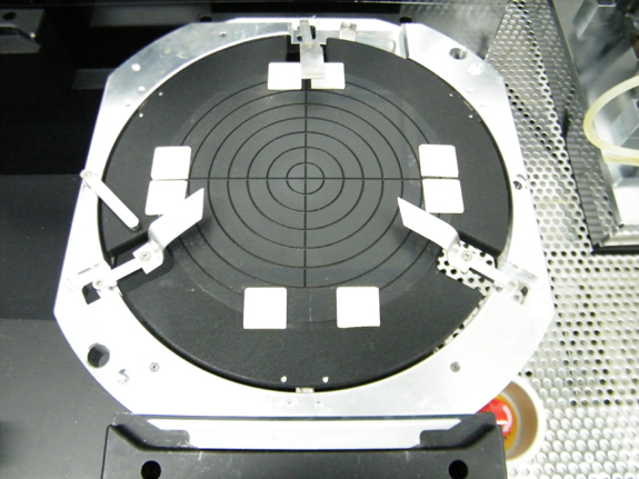
Used EVG / EV GROUP 520 #9022766 for sale
It looks like this item has already been sold. Check similar products below or contact us and our experienced team will find it for you.
Tap to zoom


Sold
ID: 9022766
Wafer Size: Up to 8"
Vintage: 2002
Bonder, up to 8"
Manual wafer load substrate bonder
Capable of fusion compression bonding
Capable of thermal compression bonding
Anodic bonding can be added at additional cost
R&D and pilot production applications
High-vacuum capable bond chamber
Auto opening of bond tool cover
Windows based control software and operation interface
Wafer size: up to 8" capable
Vacuum chuck: 8"/200mm diameter chuck
Max bond force: 7 kN
Bottom side heater: 550°C max. in 1°C steps
Temperature uniformity: ± 1.5 %
Turbo pump and controller
Roughing pump
Load / unload tool
System computer, monitor, and keyboard
Windows XP operating system
Operations manual
Can be inspected and demonstrated
2002 vintage.
EVG / EV GROUP 520 (EVG 520) is an advanced wafer bonding and lithography tool designed for a wide range of microscale and nanoscale production applications. It features an encapsulated low substrate temperature environment and an advanced thermal control equipment giving it the ability to bond wafers with ultra-thin line widths and high throughput. EV GROUP 520 also has a high precision motion control system and an automated alignment unit to ensure accuracy. In addition, the machine is equipped with a low-vacuum contour machine, giving it the capability to bond large substrates with extremely small and intricate features. This makes 520 suitable for production of photonic, optoelectronic, and sensor devices, as well as integrated circuits and complex wafer-scale structures. The die attach module of EVG / EV GROUP 520 is capable of bonding die on a wide range of substrates, including high temperature semiconductor materials. It also features an automated tape feeder, vacuum chuck clamping, and sealed heaters to ensure precise die placement and optimal temperature control. EVG 520 also contains a state-of-the-art software suite with features like die recession edges, automated layer mapping, and precision alignment. The lithography module of EV GROUP 520 is capable of printing intricate patterns down to 90 nm and with a 5mm line width. This means that it has the capability to print small and intricate circuit elements such as photonic circuits and waveguides onto a substrate. In addition, the lithography module has an advanced optical focus control tool, which enables it to maintain a consistent focus for any printed patterns. Overall, 520 is an advanced and reliable tool for production of photonics, optoelectronics, and other small scale electronics. Its features, such as its condensed environment, low substrate temperature, and precise motion control asset make it suitable for a wide range of nanoscale and microscale applications.
There are no reviews yet