Used JFP MICROTECHNIC PP5 #293820606 for sale
URL successfully copied!
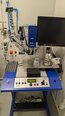
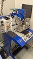
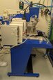
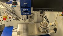
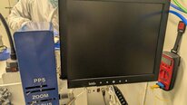
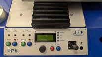
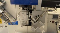
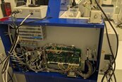
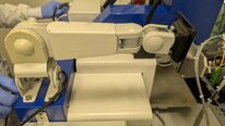
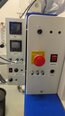
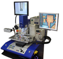
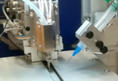

Tap to zoom

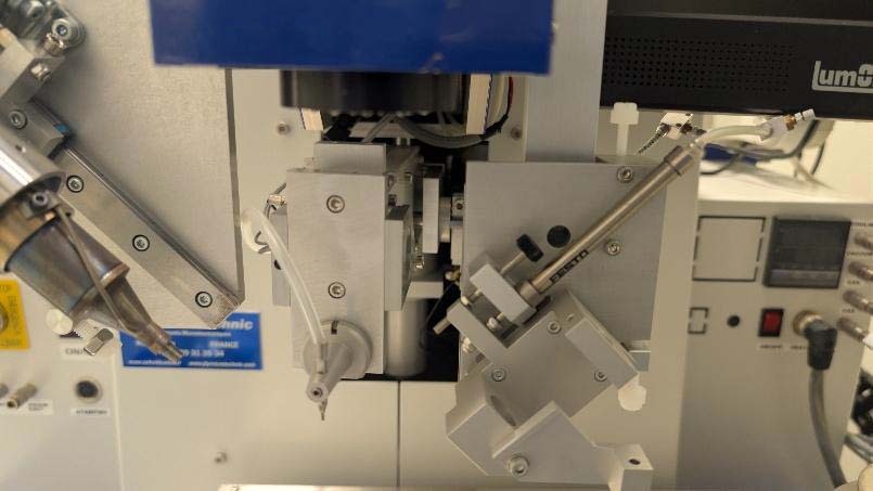
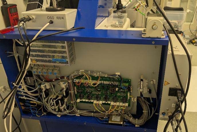
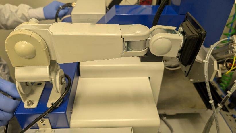
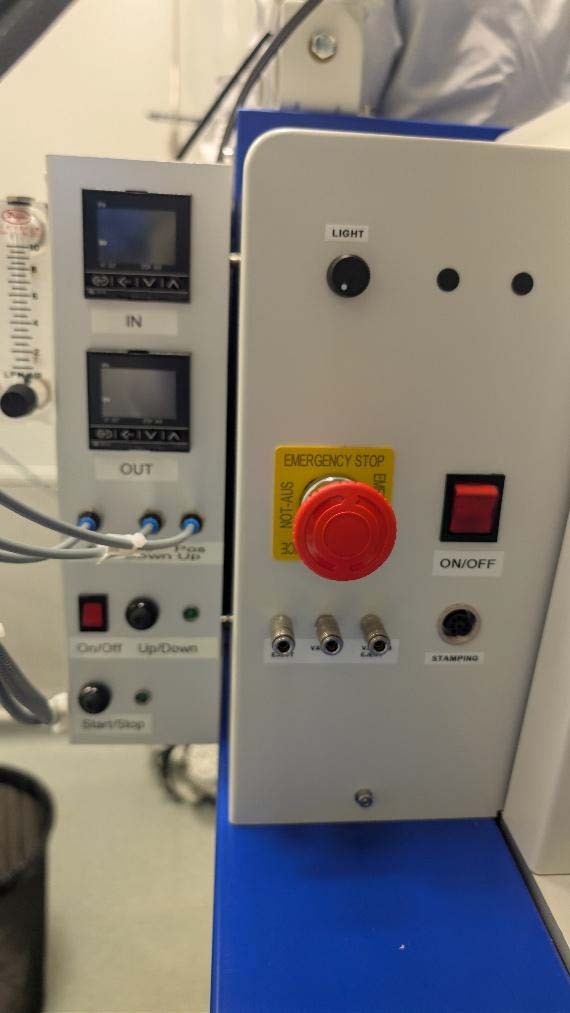
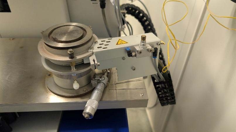
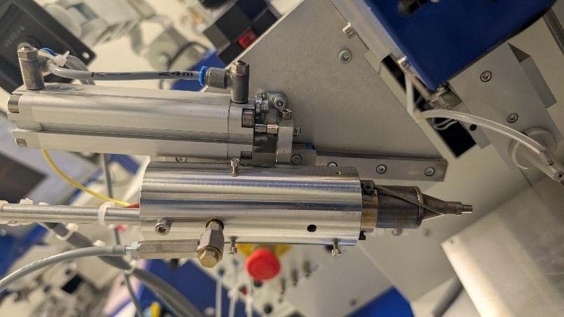
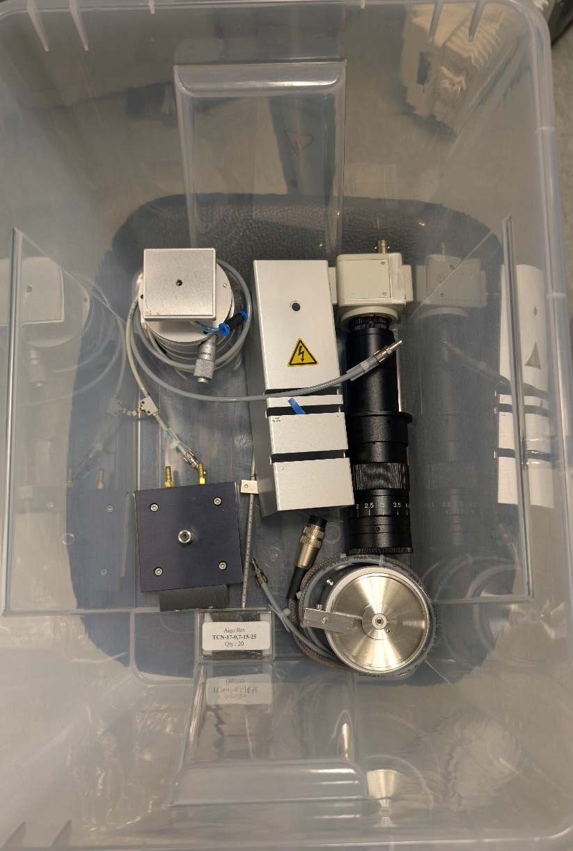
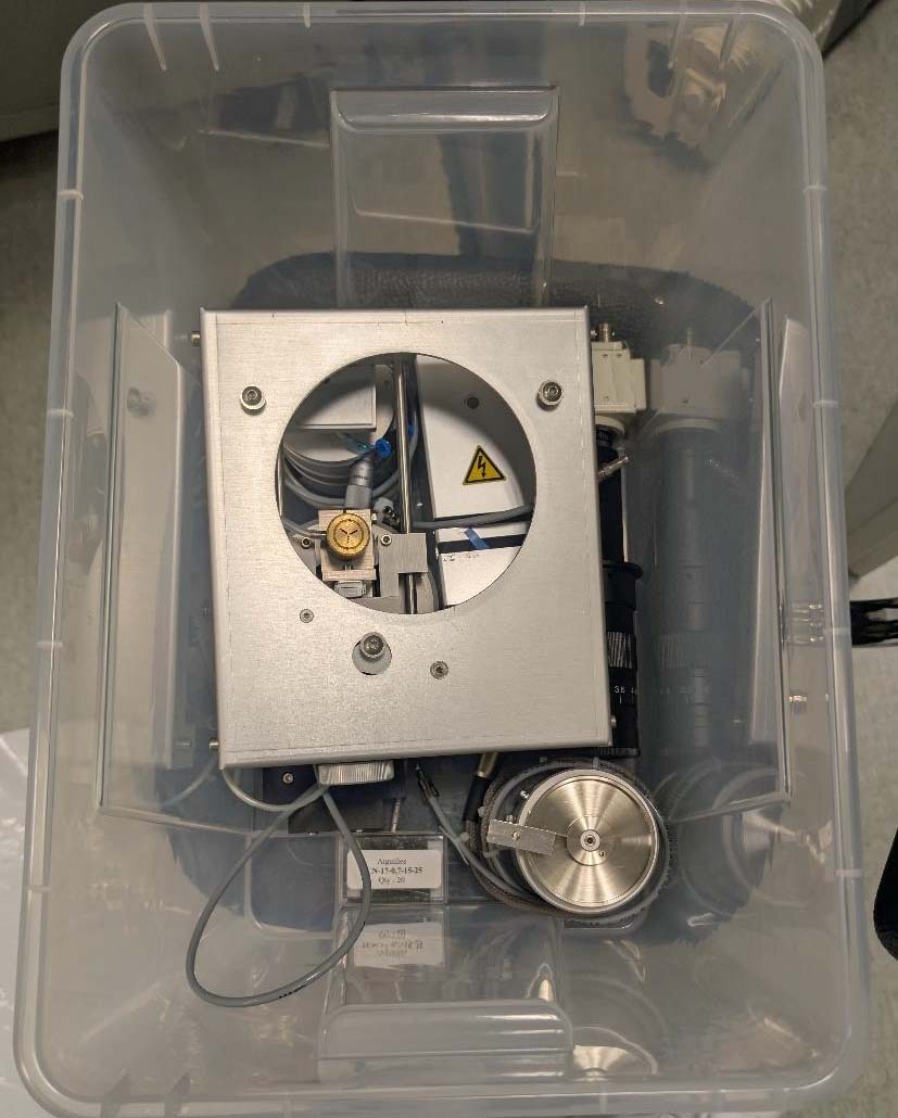

ID: 293820606
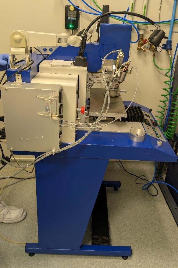
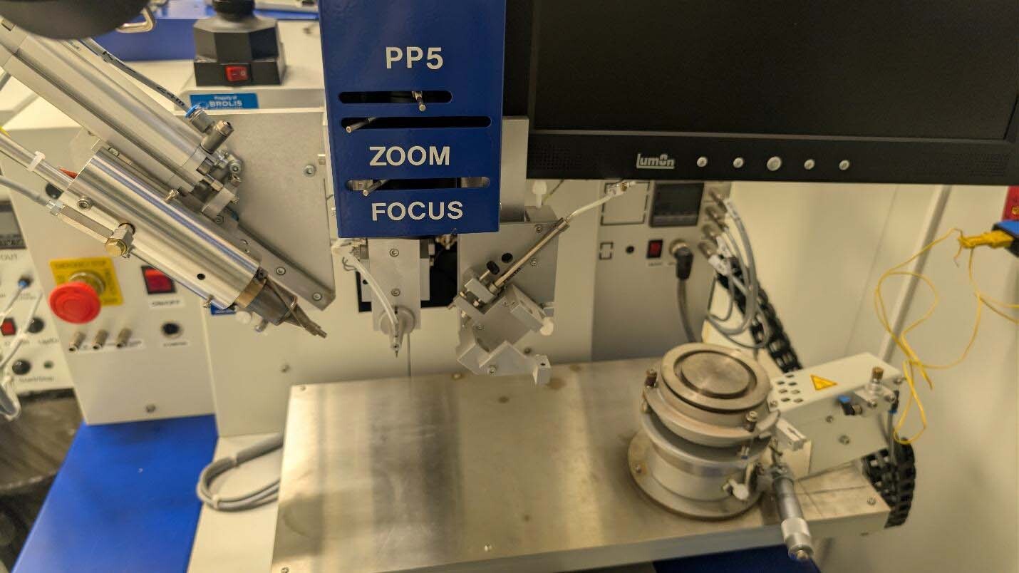
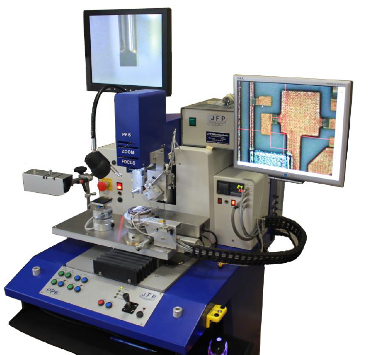
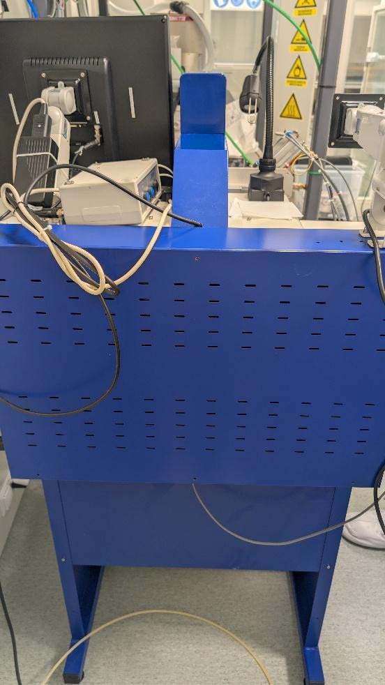
Die bonder
Process: Thermo‑sonic die bonding
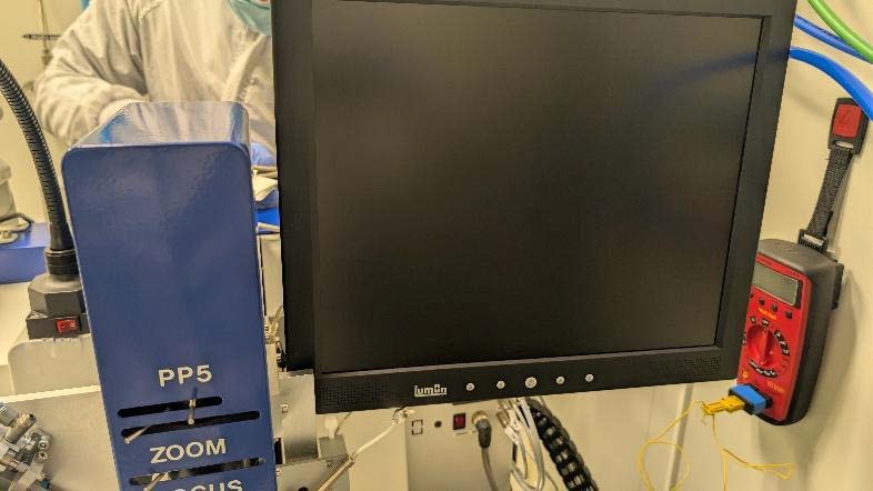
(2) Monitors
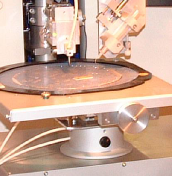
Wafer sorter
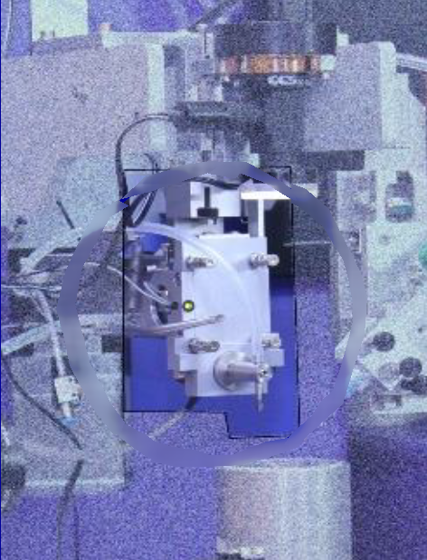
Stamping unit for epoxy / solder paste
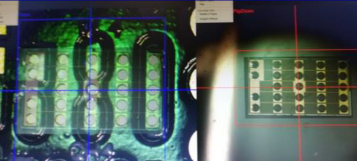
UHD Vision system
Full FoV = 2.7 mm
Standard resolution: 0,55 µm
Motorized XY tables: 260 mm × 120 mm
Resolution: 0.1 µm
TFT 22” display
High‑accuracy centering stage
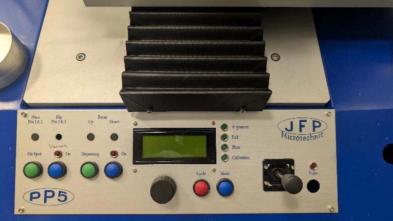
Joystick control
LED / coaxial / oblique lighting
Alignment system
Flip‑chip alignment
UV insulator
Placement accuracy: ±1 µm
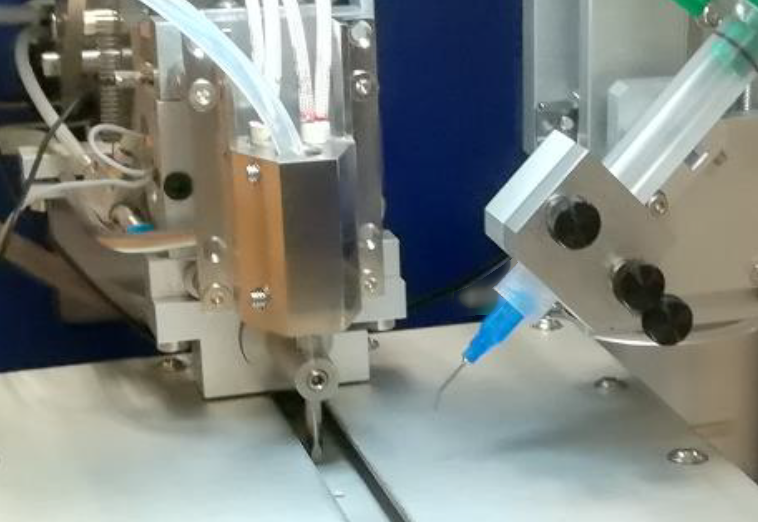
Ultrasonic head
Heated tool
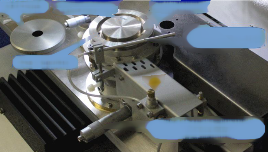
Eutectic station
Rotary stamping unit
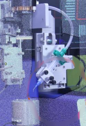
Dispensing head
Flip system
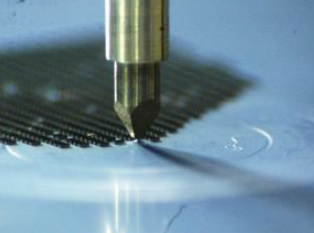
Wafer die-ejector
Small chips: 150µ
Laser diode
Laser bar
Option process camera
No touchscreen.
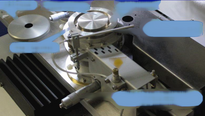
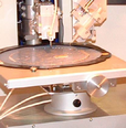
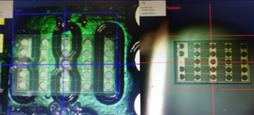
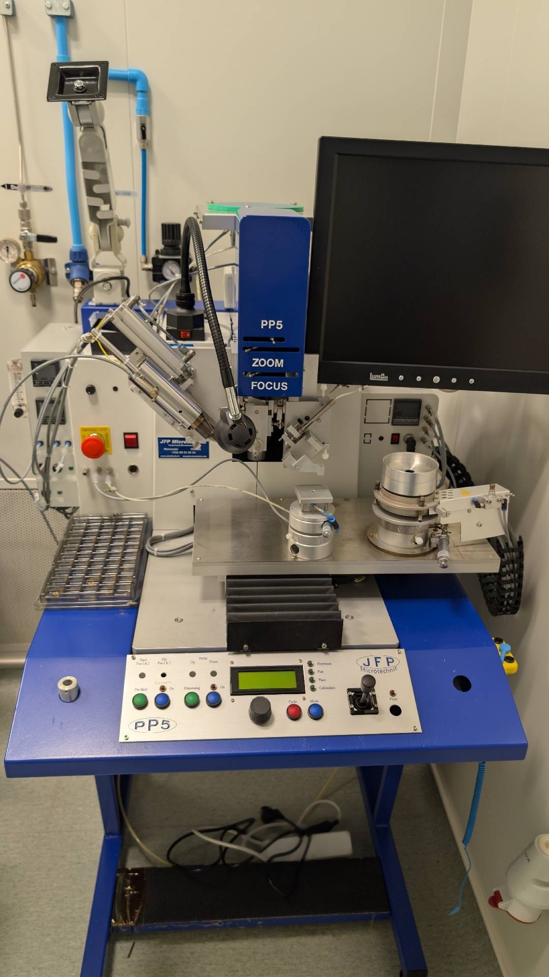
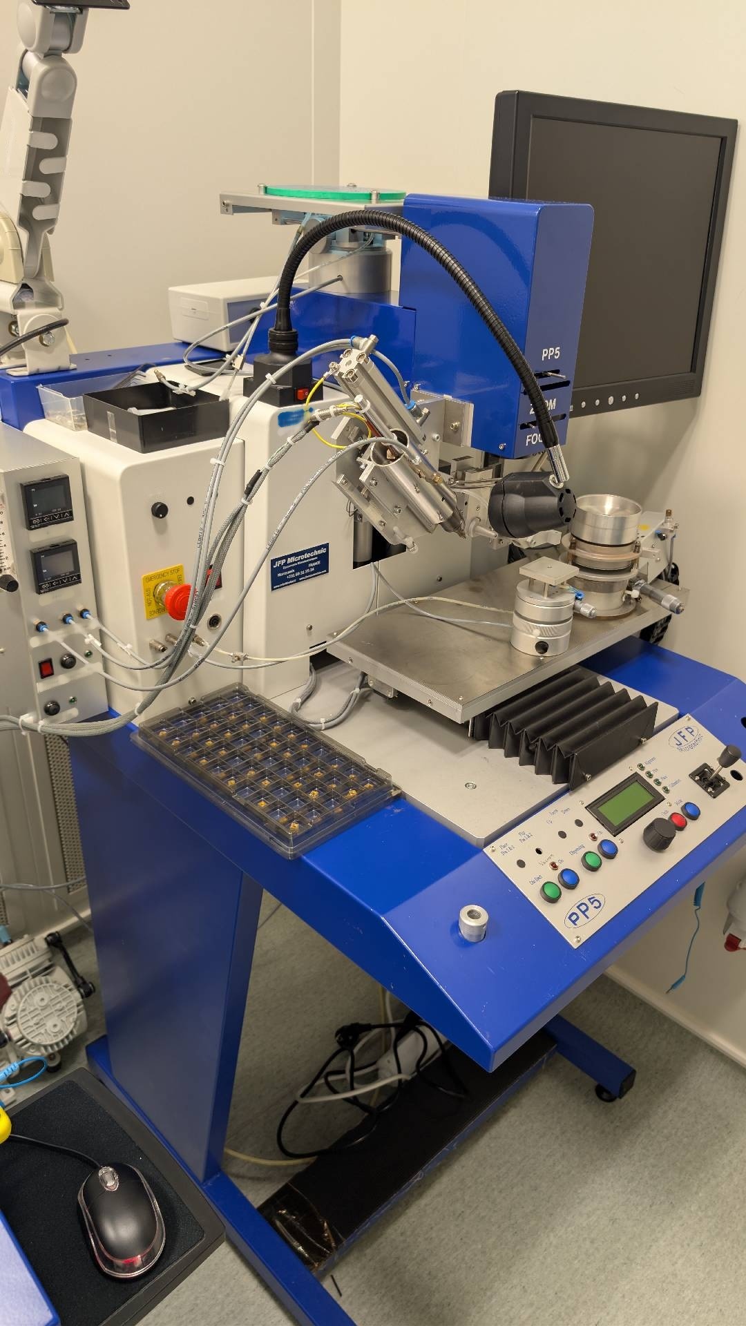
JFP MICROTECHNIC PP5 bonder is a cutting-edge microelectronics assembly equipment designed for high-precision bonding applications in the semiconductor industry. It incorporates advanced technology and features to ensure superior performance, accuracy, and reliability in bonding processes, making it an indispensable tool for semiconductor manufacturers, research laboratories, and other industries requiring microelectronics assembly. PP5 bonder is equipped with a sophisticated bonding mechanism that enables precise and controlled bonding of small components such as microchips, sensors, resistors, capacitors, and other electronic devices onto substrates with exceptional accuracy and repeatability. This capability is essential for ensuring the quality, functionality, and performance of microelectronic devices, as even the slightest deviations in bonding can lead to performance issues and product failure. One of the key features of JFP MICROTECHNIC PP5 bonder is its high-precision alignment system, which allows for the accurate positioning of components and substrates during the bonding process. This ensures that the bonding pads are perfectly aligned and in contact with each other, resulting in strong and reliable interconnections that can withstand the rigors of operation in various environments. The alignment system can be programmed and customized to accommodate different bonding configurations and requirements, making the bonder versatile and adaptable to a wide range of applications. PP5 bonder is also equipped with advanced vision systems and imaging technologies that provide real-time feedback and monitoring of the bonding process. This allows operators to visually inspect and verify the quality of the bonds, detect any defects or anomalies, and make adjustments as necessary to ensure optimal bonding results. The imaging capabilities of the bonder can capture high-resolution images of the bonding area, allowing for detailed analysis and documentation of the bonding process for quality control and traceability purposes. In addition to its advanced bonding capabilities, JFP MICROTECHNIC PP5 bonder is designed for ease of use and operational efficiency. It features an intuitive user interface with a touchscreen display that allows operators to easily set up and control the bonding process, monitor performance metrics, and access diagnostic information. The bonder can be integrated into automated production lines and controlled remotely for seamless operation and process optimization. Moreover, PP5 bonder is built with robust construction and high-quality materials to ensure durability and longevity in demanding manufacturing environments. It is designed to withstand continuous use and perform reliably over an extended period, requiring minimal maintenance and servicing to keep it operating at peak efficiency. The bonder's compact footprint allows for efficient use of space in production facilities and research laboratories, optimizing workflow and productivity. Overall, JFP MICROTECHNIC PP5 bonder is a state-of-the-art microelectronics assembly equipment that offers unparalleled precision, accuracy, and reliability in bonding applications. Its advanced features, high-performance capabilities, and user-friendly design make it an essential tool for achieving high-quality and reliable microelectronic assemblies in various industries. With PP5 bonder, manufacturers and researchers can achieve superior bonding results, accelerate production processes, and ensure the performance and reliability of their microelectronic devices.
There are no reviews yet