Used GASONICS / NOVELLUS Aura 1000 #293586844 for sale
URL successfully copied!
Tap to zoom
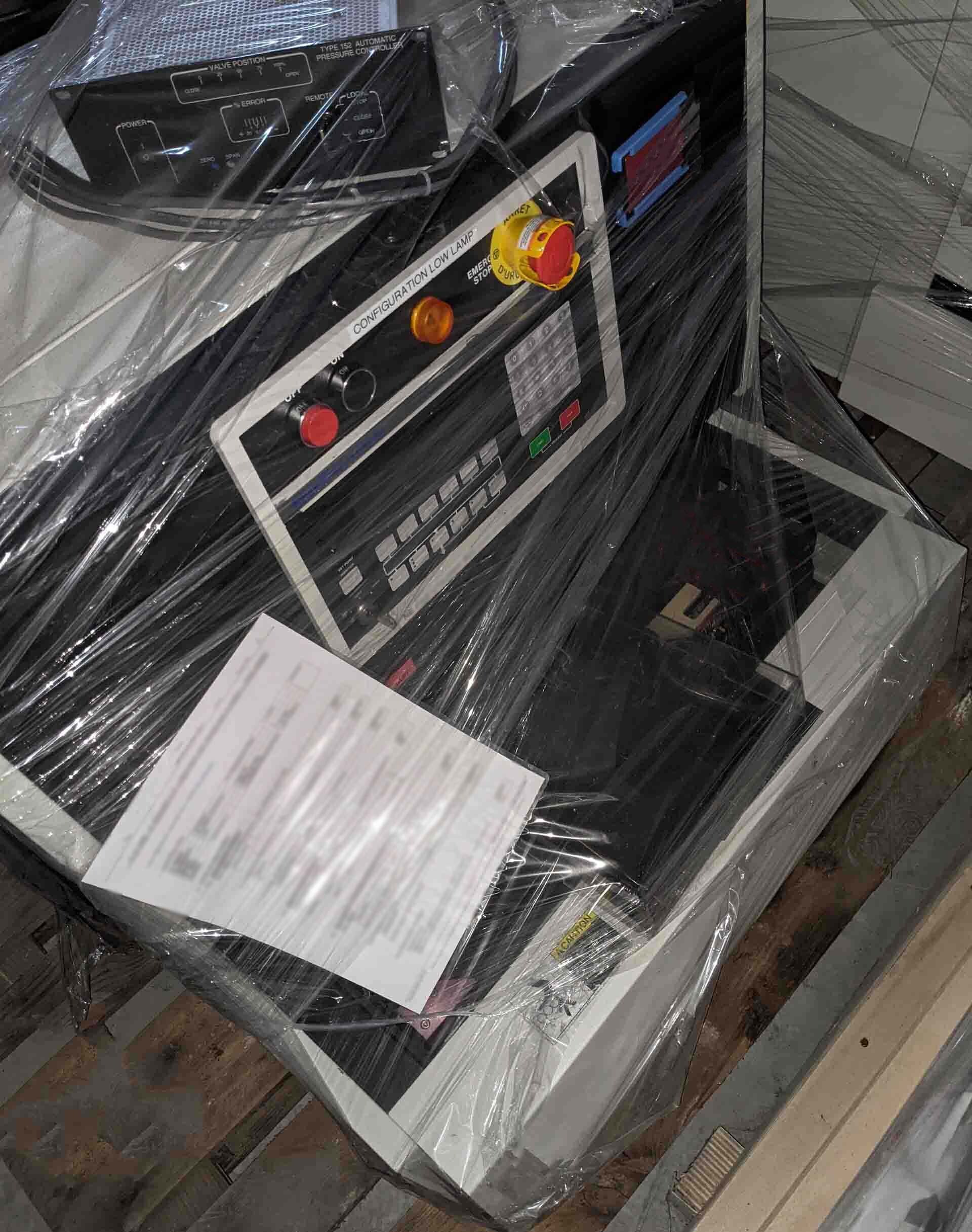

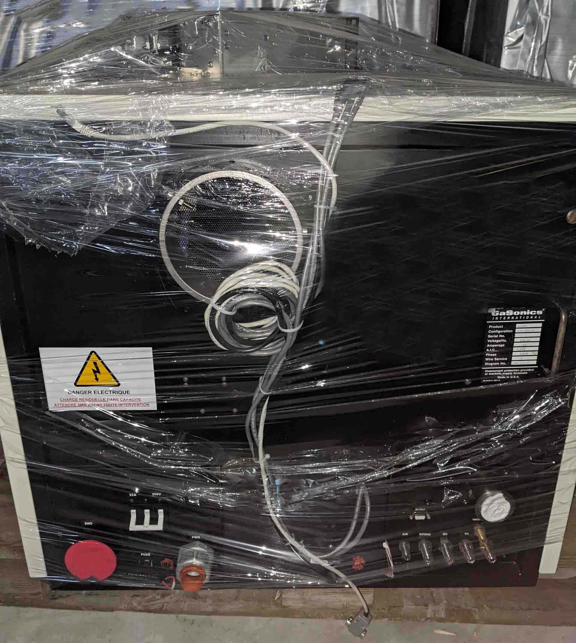

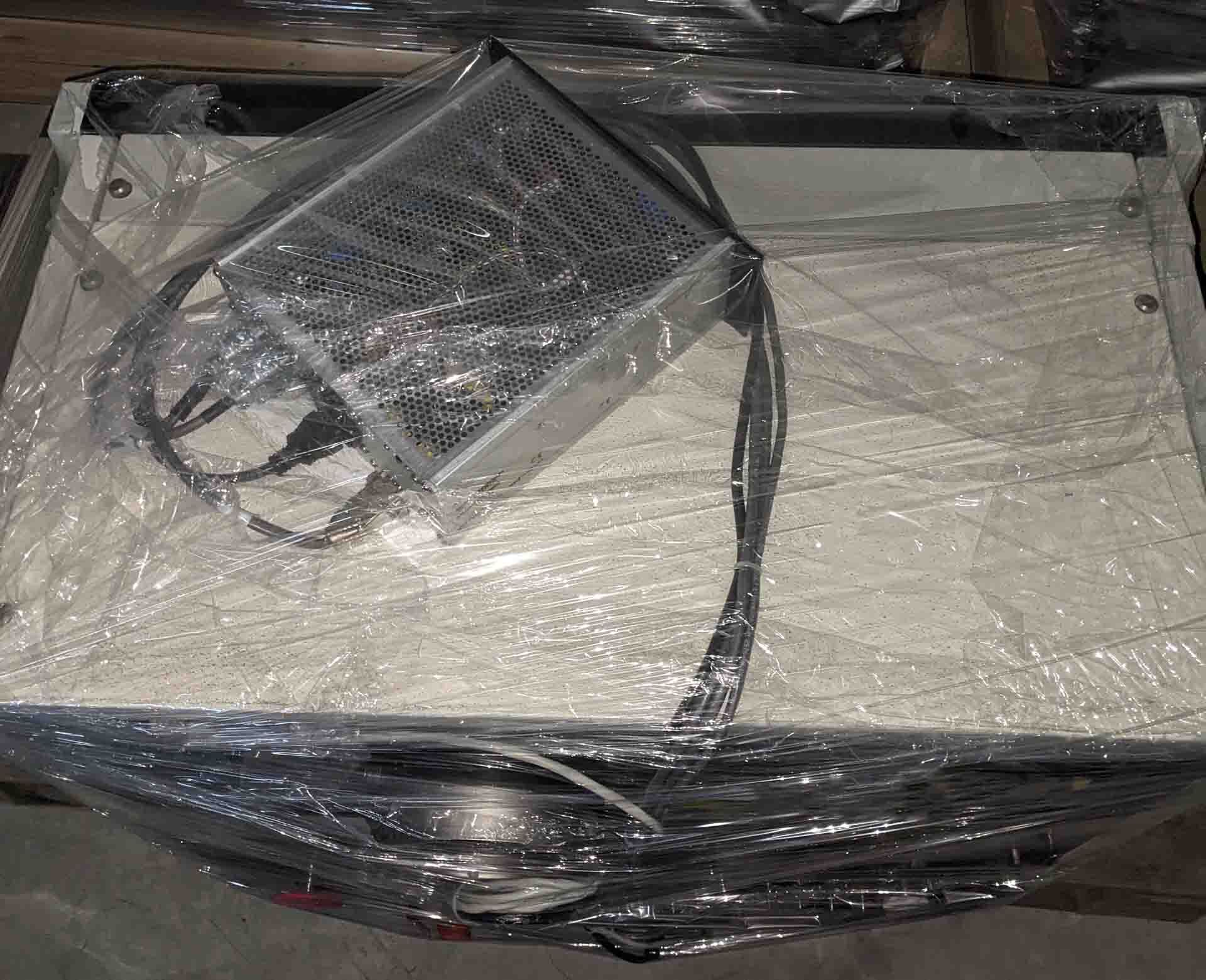

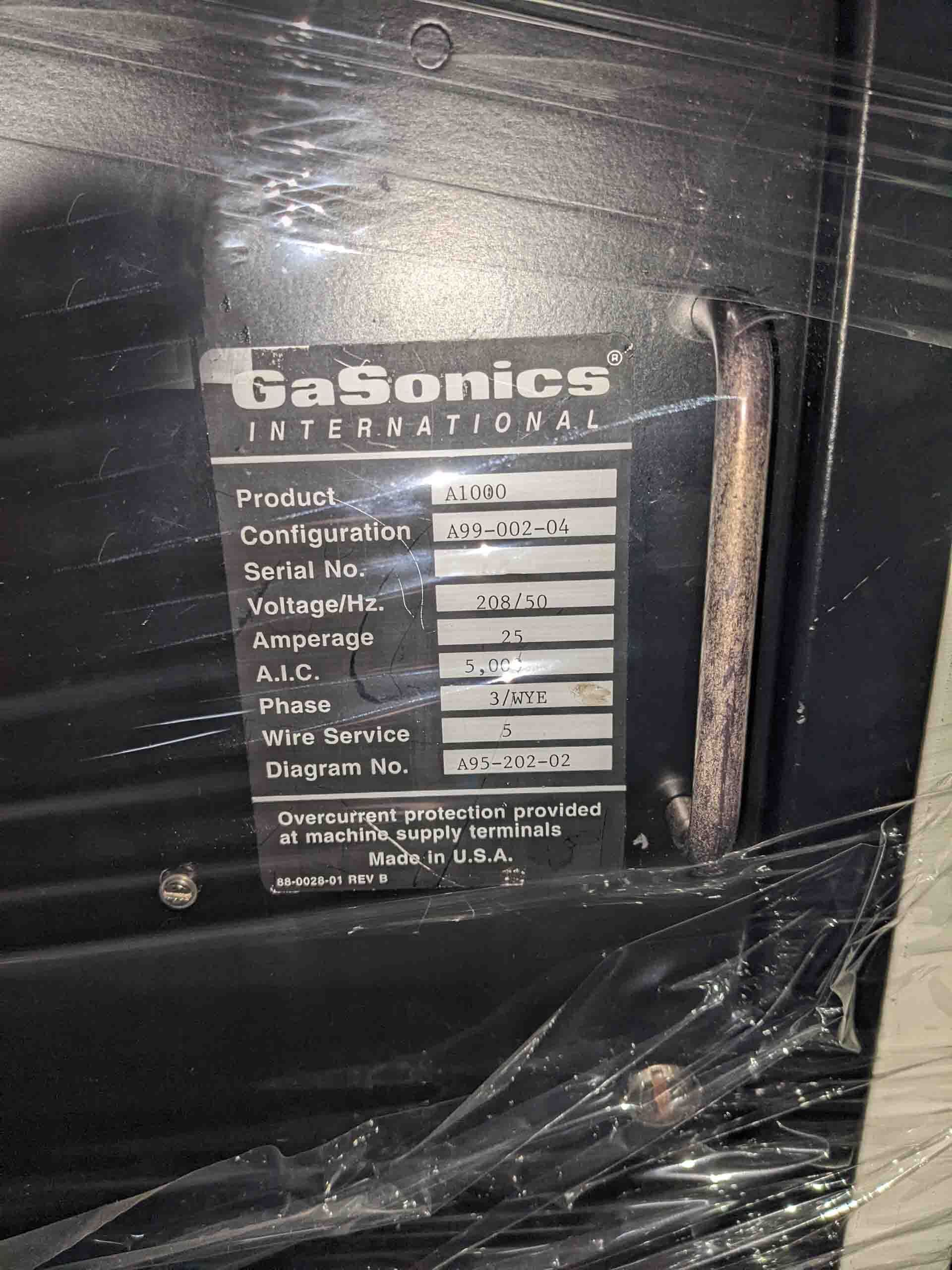

GASONICS/GASONICS / NOVELLUS Aura 1000 is an etcher/asher used in semiconductor device manufacturing to create flat surfaces and well-defined device structures on a substrate. GASONICS Aura 1000 is composed of three main components: a gas delivery module, a power supply, and a physical platform. It is designed to produce uniform, high-quality results for a variety of substrate materials, including silicon, quartz, and nitride. The gas delivery module enables a wide range of process chemistries and material specific ablation processes. It features independent control of up to four precursor gases and several argon support gases, allowing flexibility with unique geometries and layer numbers. The typical flow rates range from 0.1 to 10 SLPM, enabling accurate gas flow control while reducing the amount of necessary reagents. A pressure stabilizer is capable of controlling the pressure inside the chamber to regulate the etching rate and minimize the formation of defects on the surface. The power supply provides reliable, high-precision power delivery with excellent temperature stability to the device. It possesses pulse control capability with a wide range from 10 to 100 µs. The power supply also allows for high power delivery, up to 400 watts, with adjustable pulse repetition rates and frequency. The physical platform of NOVELLUS Aura 1000 is designed for stability, robustness and accuracy. It measures 40" in width, 40" in length, and 55" in height, and is mounted to an isolated base for vibration control, reducing wafer breakage due to movement. It also features a large particle free process chamber, with a diameter of 20", enabling larger wafer sizes to be processed at once. In conclusion, NOVELLUS/Aura 1000 is an etcher/asher specifically designed for semiconductor device manufacturing. It offers flexibility with material specific ablation processes and reliable, high-precision power delivery with excellent temperature stability. Additionally, its large particle-free process chamber allows for larger wafers to be processed with greater accuracy and stability, resulting in well-defined device structures.
There are no reviews yet

