Used LAM RESEARCH 660-300316-007 #293765709 for sale
URL successfully copied!
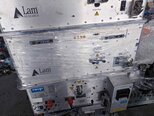
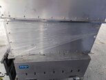
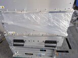
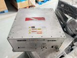
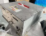
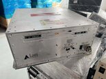
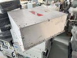
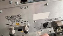

Tap to zoom
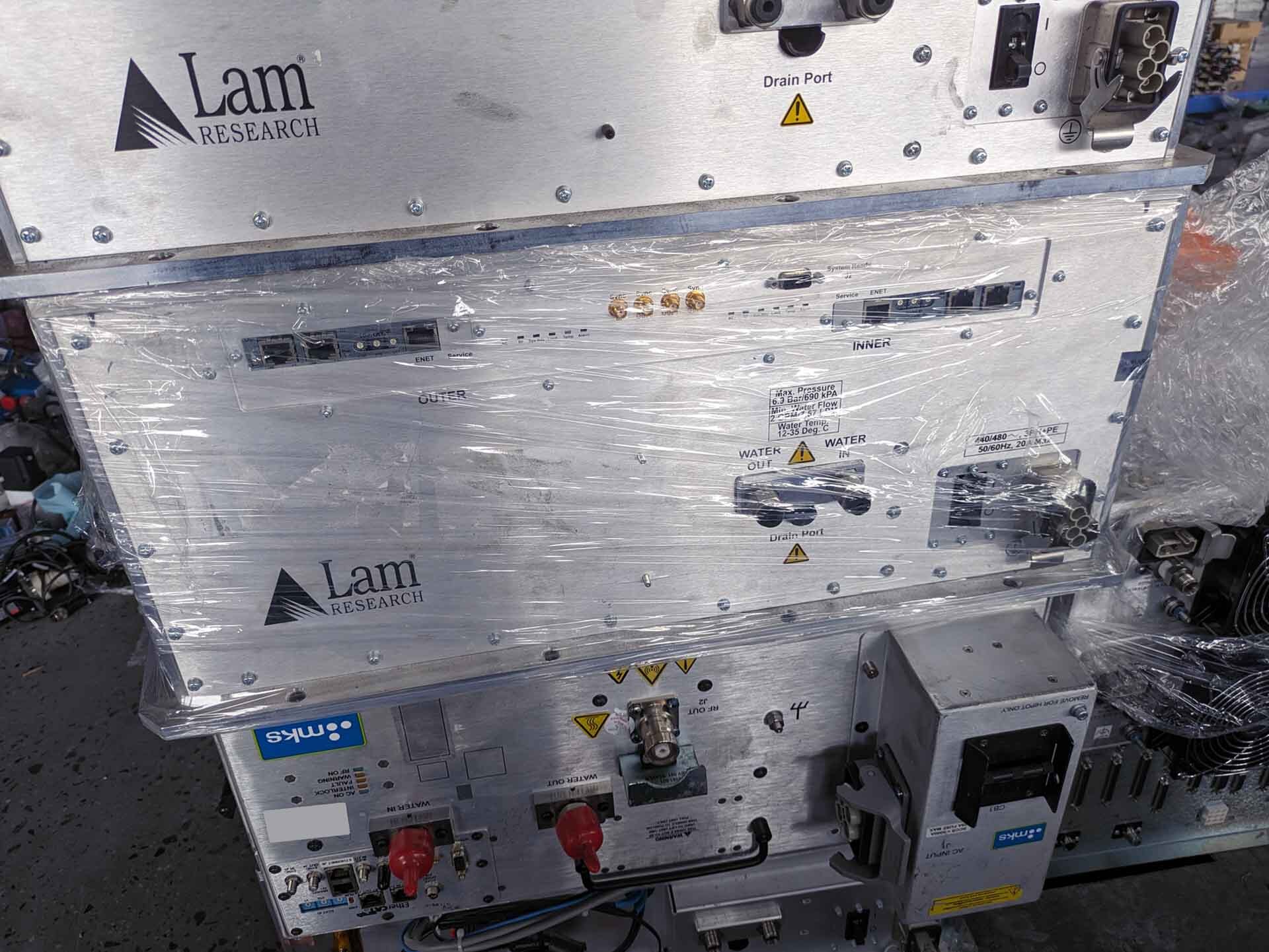

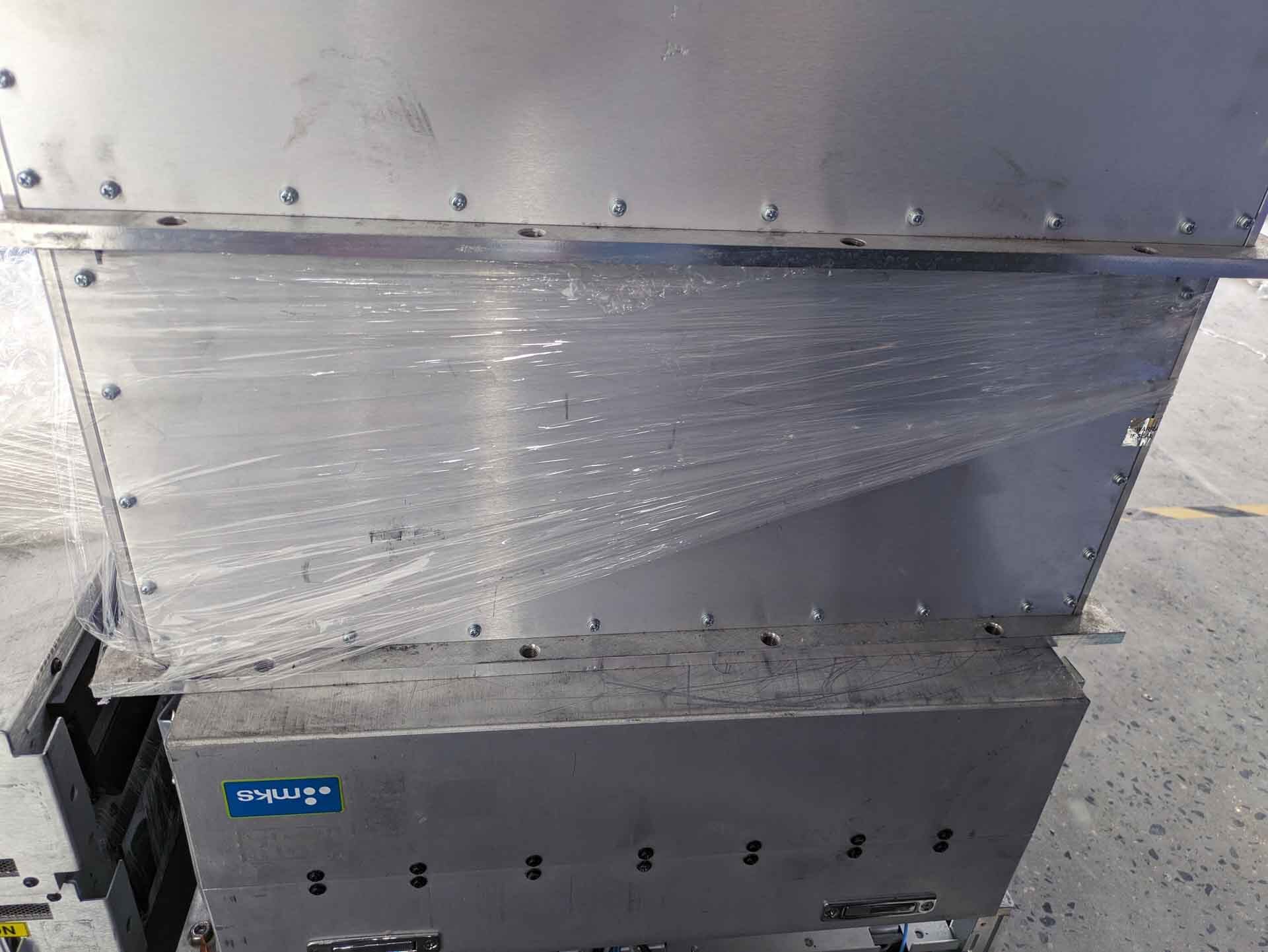
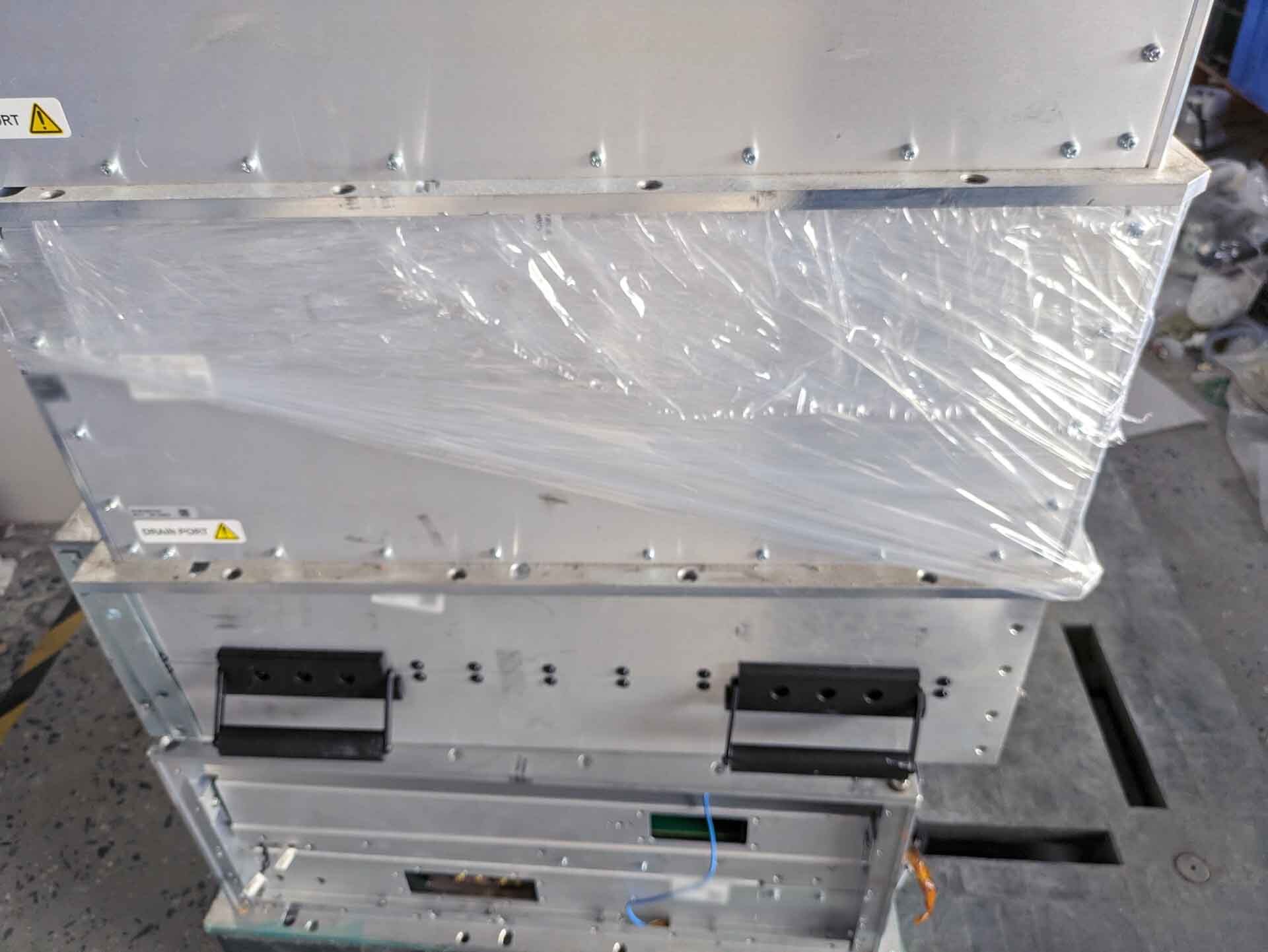
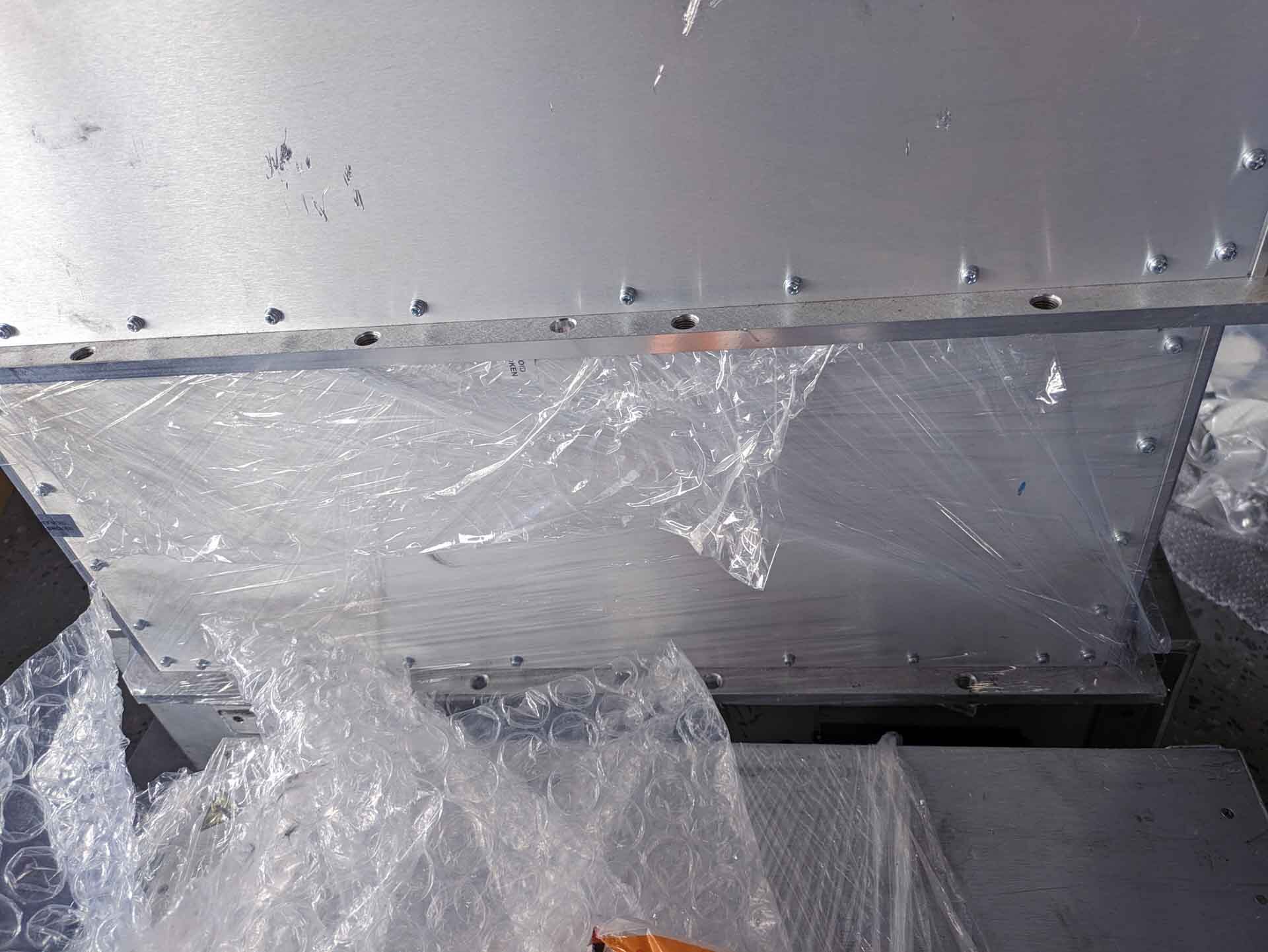
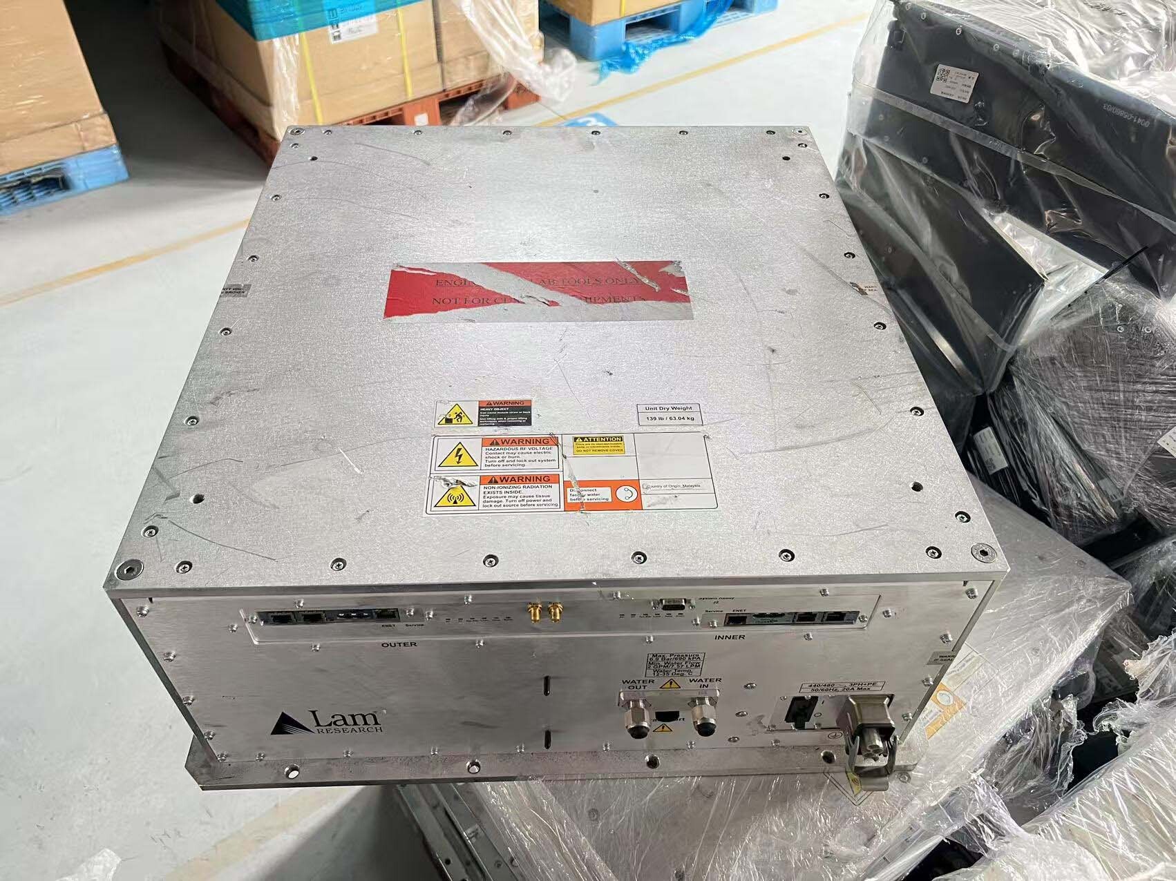
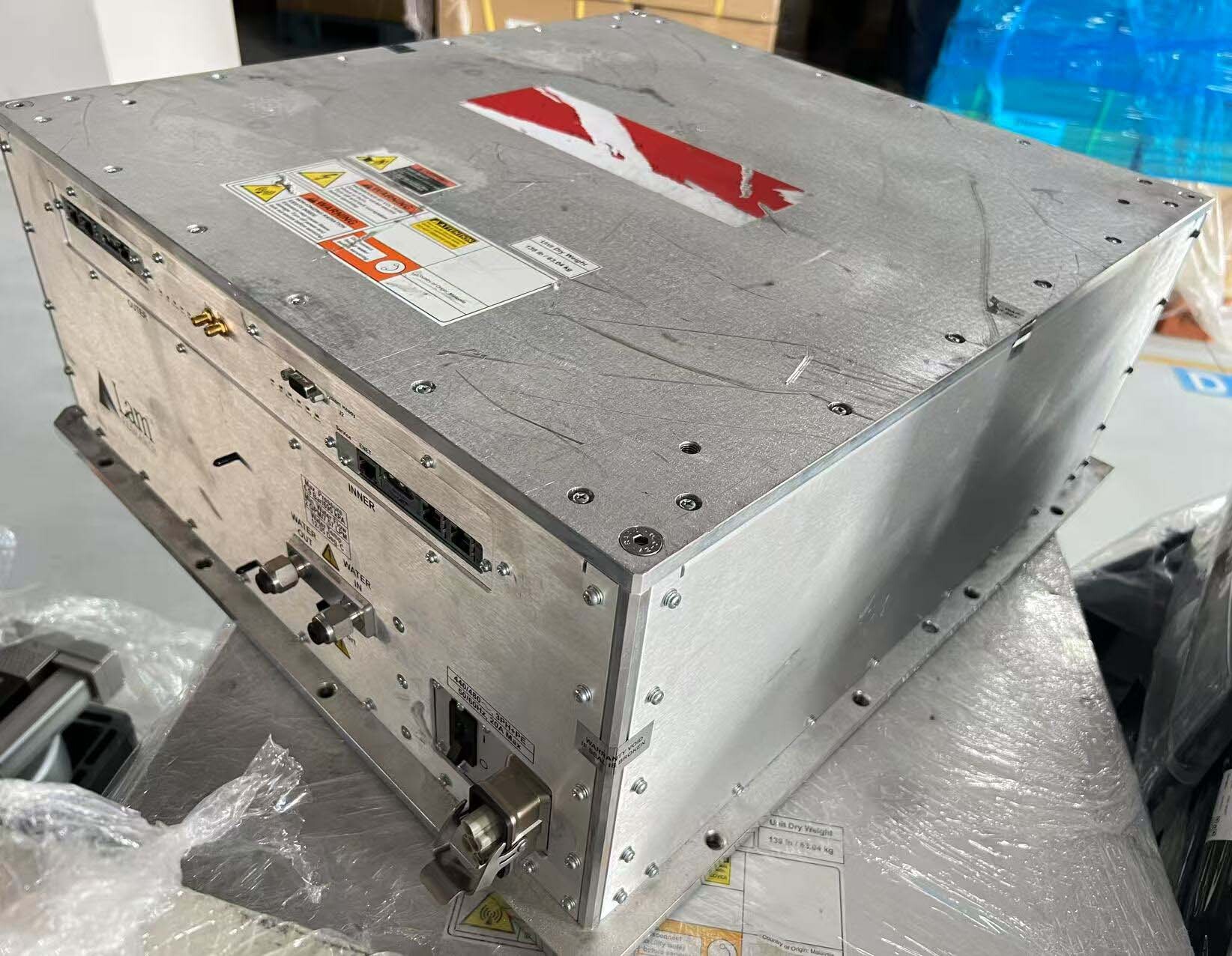
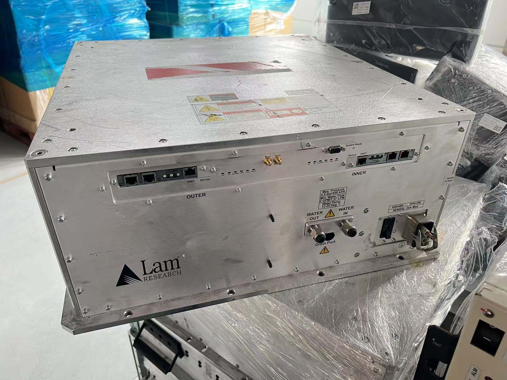
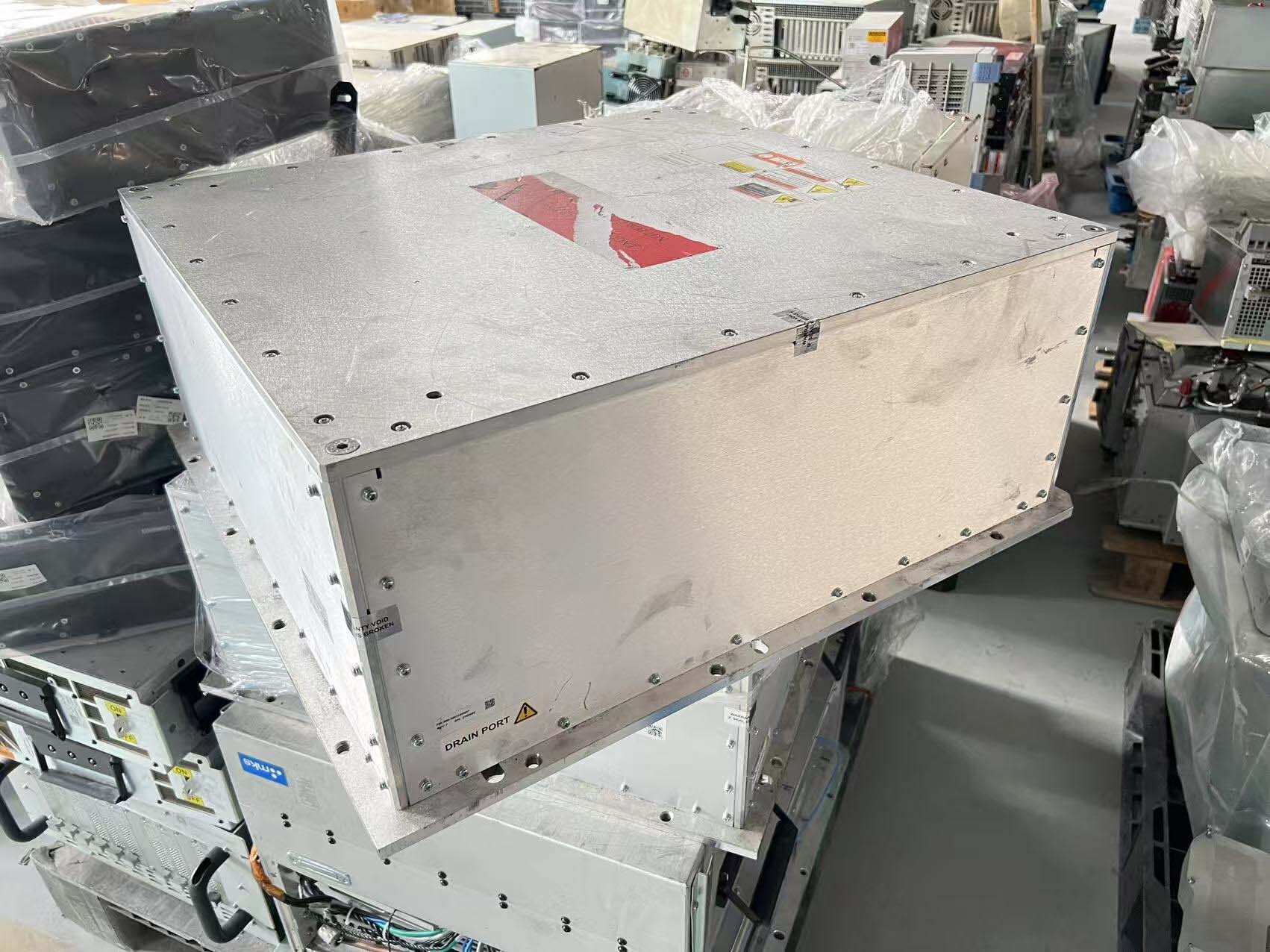
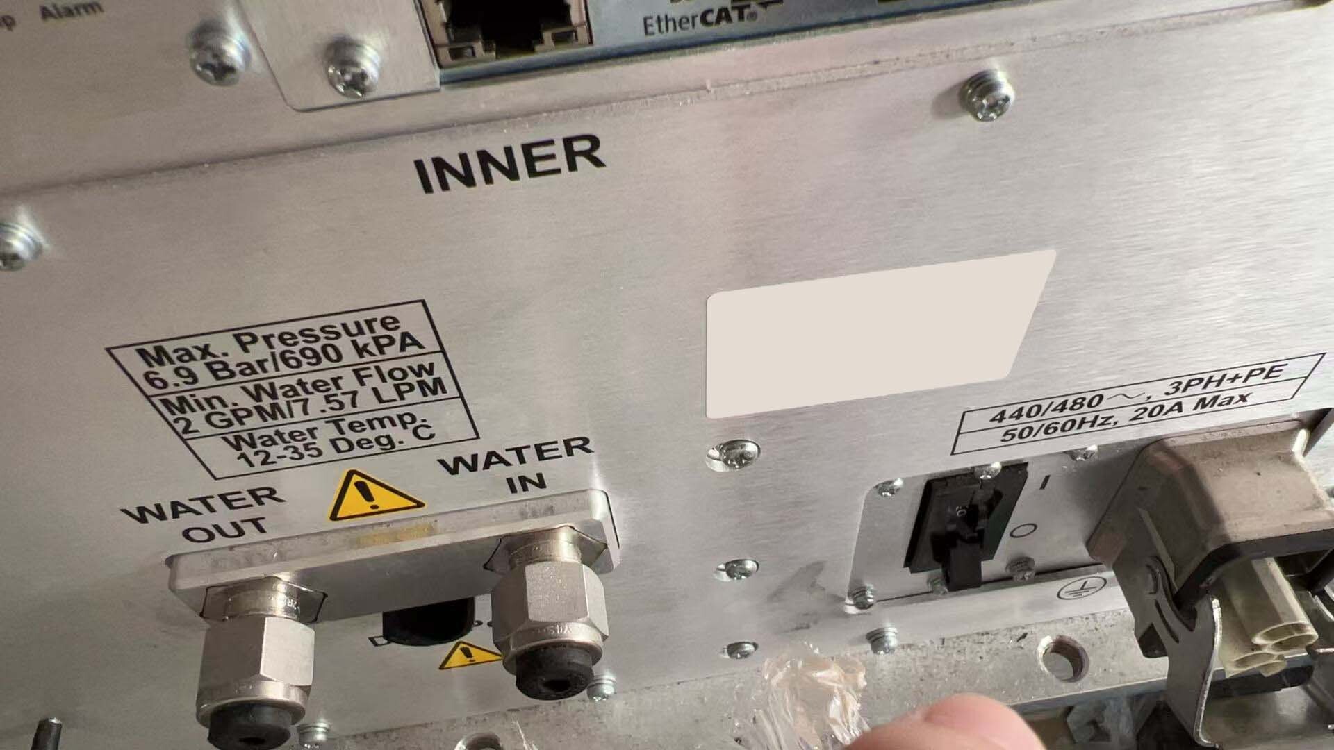
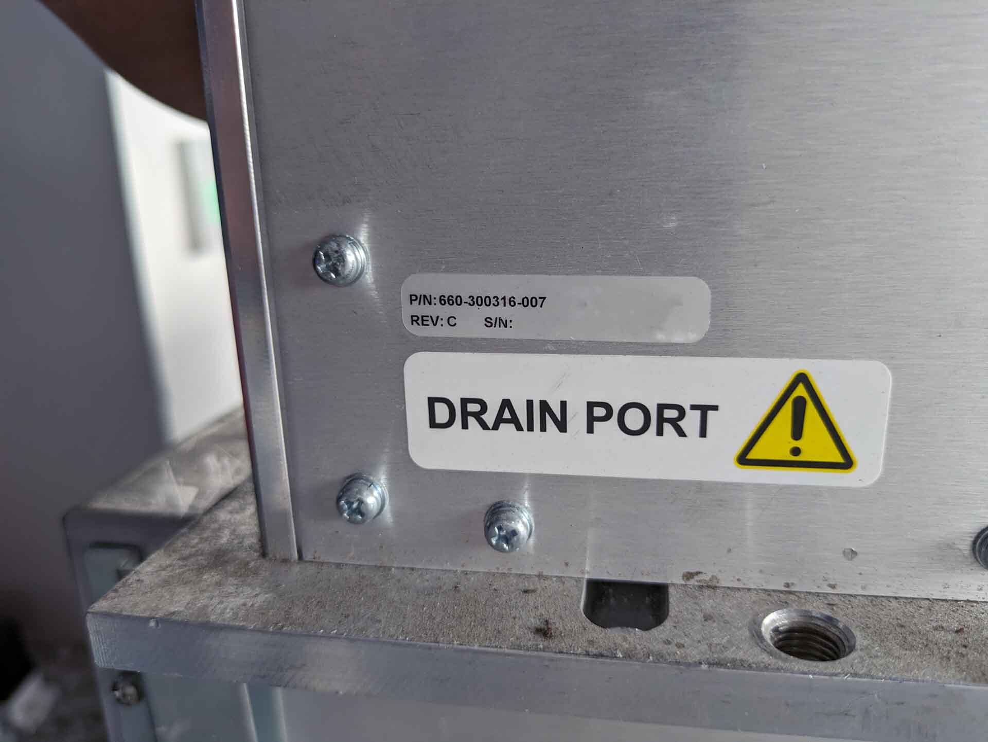
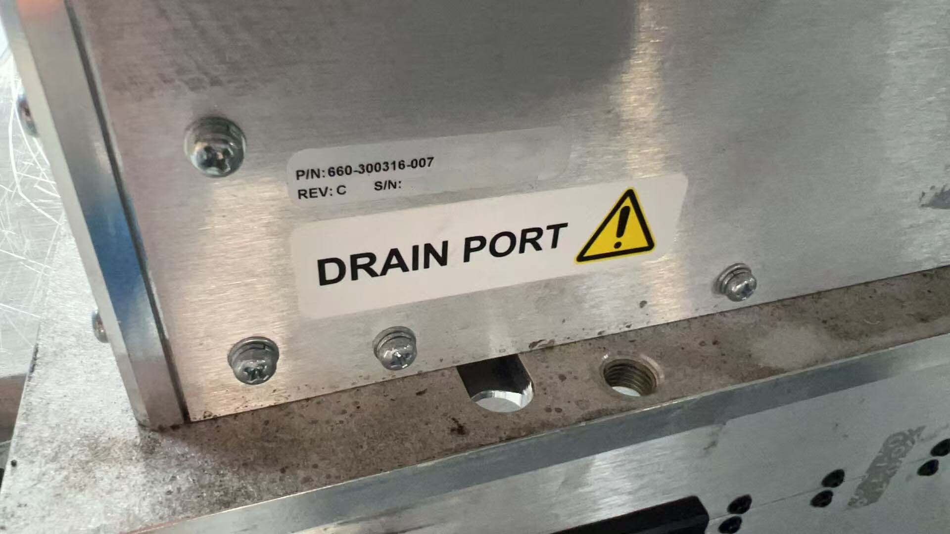
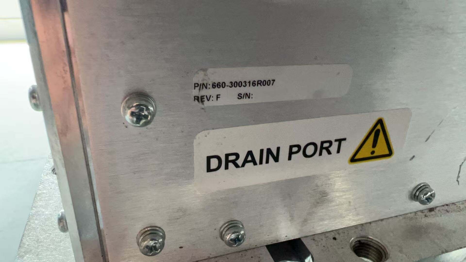
ID: 293765709
LAM RESEARCH 660-300316-007, also known as an etcher or asher, is a highly advanced semiconductor manufacturing equipment designed to etch and clean wafers used in the production of integrated circuits and other microelectronic devices. This innovative equipment employs a combination of plasma-based technologies to precisely remove material from the wafer surface, ensuring high process repeatability and uniformity across a range of substrates. At the heart of the LAM 660-300316-007 lies a sophisticated plasma etching chamber that utilizes high-frequency RF power to create a plasma environment within the processing chamber. The plasma generated in this system consists of reactive gases, such as fluorine-based compounds, that chemically react with the material on the wafer surface, selectively etching away unwanted layers with high precision and control. The chamber is carefully designed to optimize gas flow dynamics, temperature control, and uniformity of the plasma distribution, ensuring consistent etching performance across the entire wafer surface. One of the key features of the LAM LAM RESEARCH 660-300316-007 is its advanced process control capabilities, which allow operators to fine-tune etching parameters such as gas composition, pressure, power settings, and process time to achieve the desired etch profile and selectivity. The unit is equipped with intelligent monitoring and feedback mechanisms that continuously track process performance in real-time, enabling automatic adjustments to maintain process stability and repeatability. This level of control is essential for achieving tight tolerances and meeting strict semiconductor industry standards for device performance and yield. In addition to its etching capabilities, the LAM 660-300316-007 can also function as an asher, a process used to remove organic contaminants from the wafer surface prior to etching. The machine is equipped with specialized cleaning recipes and gas chemistries that efficiently strip away photoresist and other organic residues without damaging the underlying substrate. By integrating etching and ashing functionalities in a single platform, the LAM LAM RESEARCH 660-300316-007 offers manufacturers a versatile solution for streamlining their wafer processing workflows and reducing overall production costs. The LAM 660-300316-007 is built upon a robust and reliable platform that is engineered for high throughput and uptime, making it a cost-effective solution for high-volume semiconductor manufacturing facilities. The tool features a modular design that allows for easy maintenance and servicing, minimizing downtime and enabling quick tool reconfiguration for different process requirements. Additionally, the asset is compatible with industry-standard wafer sizes and can accommodate various wafer materials, making it a versatile tool for a wide range of semiconductor applications. Overall, the LAM LAM RESEARCH 660-300316-007 represents the pinnacle of plasma etching and asher technology, offering semiconductor manufacturers a powerful and flexible solution for achieving precise and repeatable wafer processing. With its advanced process control capabilities, intelligent monitoring systems, and robust design, this model is poised to drive innovation and productivity in the ever-evolving semiconductor industry.
There are no reviews yet