Used LAM RESEARCH 839-101612-885 #293751480 for sale
URL successfully copied!
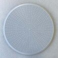
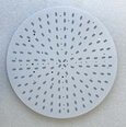
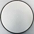
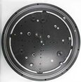
Tap to zoom
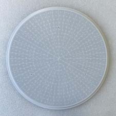

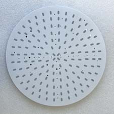
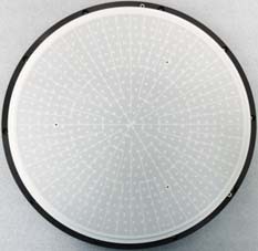
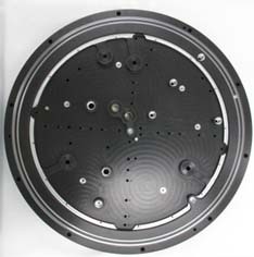
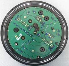
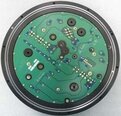
LAM RESEARCH 839-101612-885 is a highly advanced etcher/asher equipment designed for semiconductor processing applications. This equipment plays a critical role in the production of integrated circuits by etching and cleaning semiconductor wafers to create intricate microstructures and patterns. 839-101612-885 is a cutting-edge tool that offers precise process control, advanced plasma cleaning capabilities, and exceptional reliability to meet the demanding requirements of the semiconductor industry. LAM RESEARCH 839-101612-885 features a sophisticated design that incorporates state-of-the-art plasma technology for high-quality etching and ashing processes. The system is equipped with advanced RF plasma sources, gas delivery systems, and chamber design to optimize process uniformity, repeatability, and throughput. The tool is capable of handling a wide range of wafer sizes, from small pieces to large 300mm wafers, making it a versatile solution for various semiconductor manufacturing needs. One of the key features of 839-101612-885 is its advanced process control capabilities, which allow users to precisely adjust and monitor key parameters such as gas flow rates, pressure, temperature, and RF power levels. This level of control enables users to achieve precise etch rates, selectivity, and uniformity across the wafer surface, resulting in high-quality and repeatable process results. The unit also offers real-time monitoring and data logging features, allowing operators to track process performance and make adjustments on the fly for optimal process outcomes. In addition to its etching capabilities, LAM RESEARCH 839-101612-885 is also equipped with advanced ashing functionalities for the removal of photoresist and other organic contaminants from semiconductor wafers. The machine uses a combination of plasma chemistry and temperature control to ensure thorough and efficient ashing processes while minimizing damage to the underlying substrate. This capability is crucial for removing residues and contaminants from the wafer surface, enabling clean and defect-free processing steps in subsequent manufacturing stages. The chamber design of 839-101612-885 is engineered for optimal gas flow and plasma uniformity, ensuring consistent process results across the entire wafer surface. The tool features a robust vacuum asset for rapid pump-down and stable process conditions, as well as precise temperature control to support a wide range of processing temperatures. The tool is also equipped with advanced endpoint detection capabilities to ensure accurate process timing and endpoint determination for precise process control and repeatability. Overall, LAM RESEARCH 839-101612-885 is a state-of-the-art etcher/asher model that offers advanced plasma processing capabilities, precise process control, and superior reliability for semiconductor manufacturing applications. With its versatile design, advanced features, and robust performance, this tool is well-suited for a wide range of etching and ashing processes in semiconductor fabrication facilities. The equipment's innovative technology and advanced capabilities make it an essential tool for achieving high-quality and reliable processing results in the production of cutting-edge semiconductor devices.
There are no reviews yet