Used NOVELLUS Gamma 2130 #9377872 for sale
URL successfully copied!
Tap to zoom
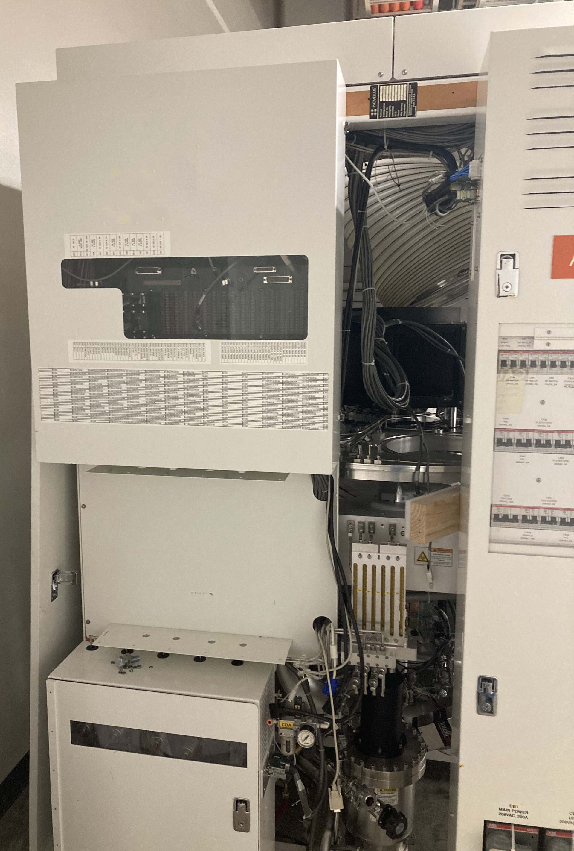

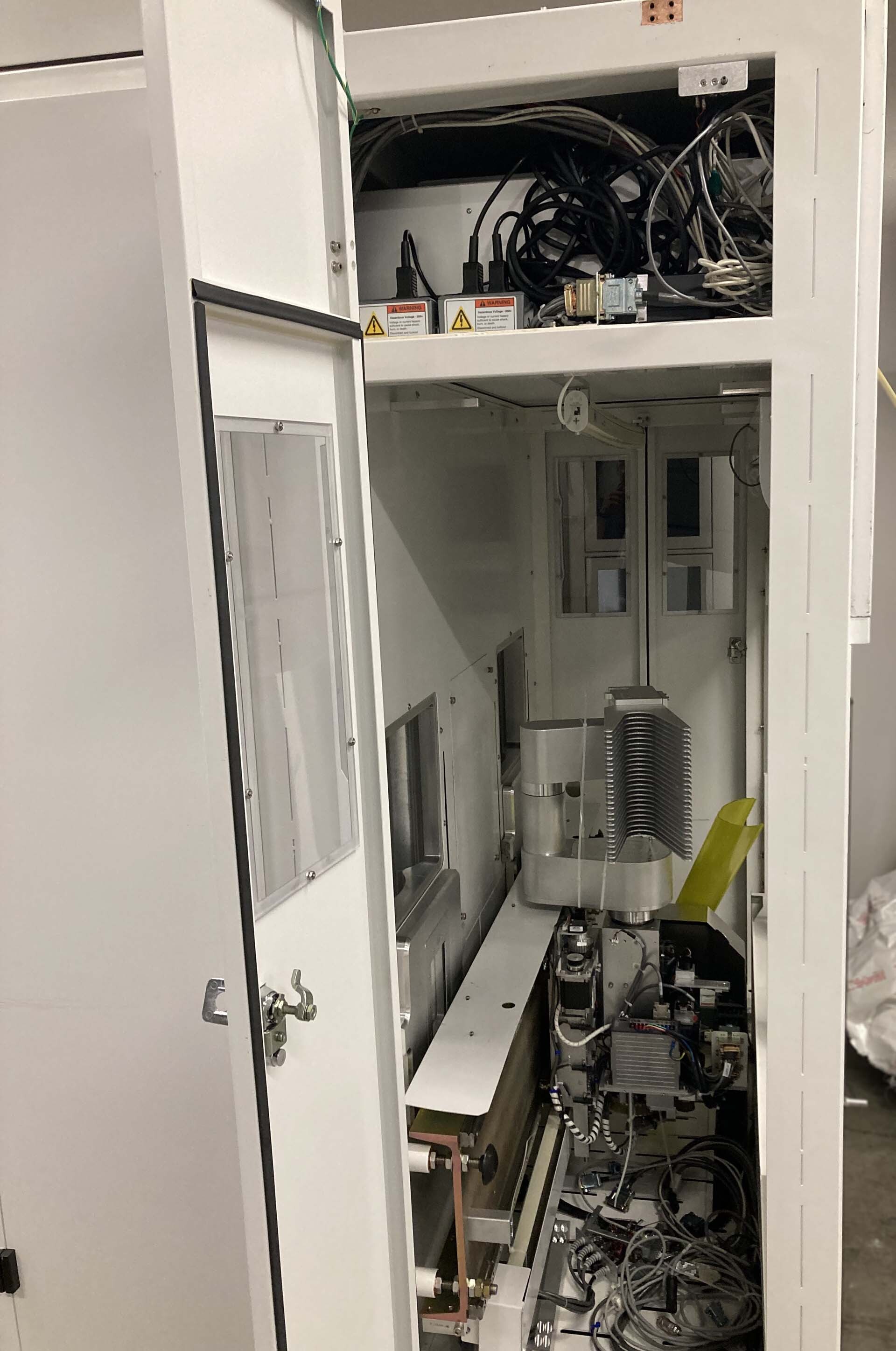

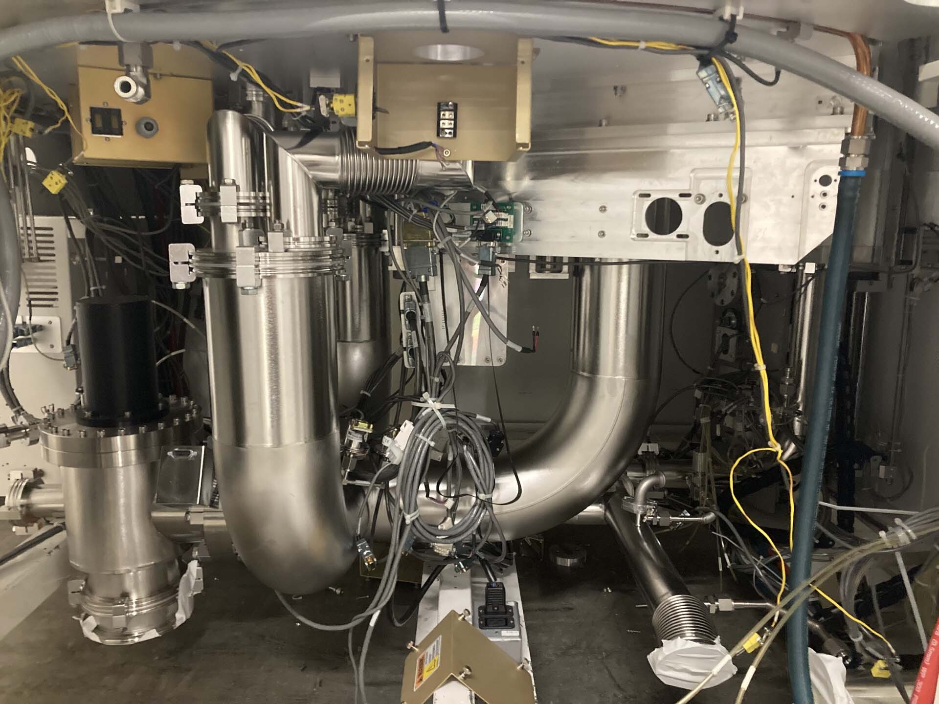

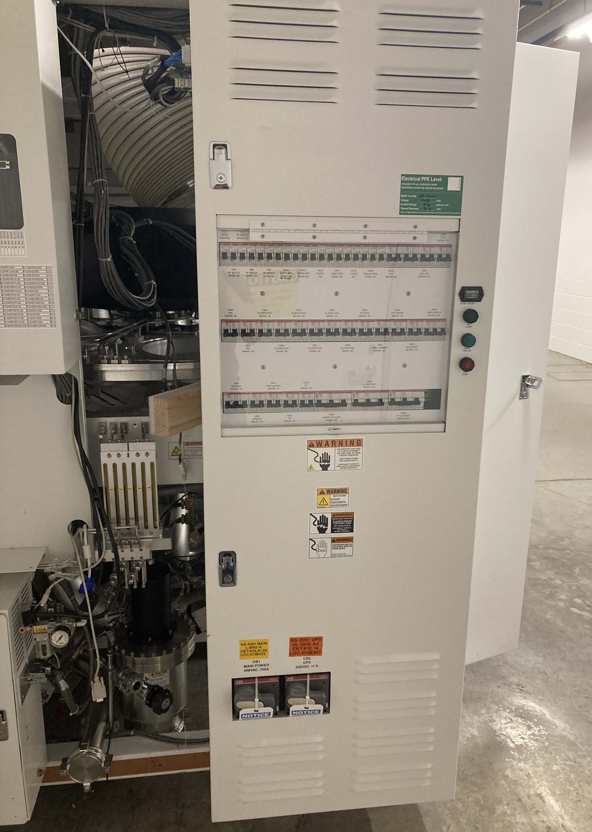

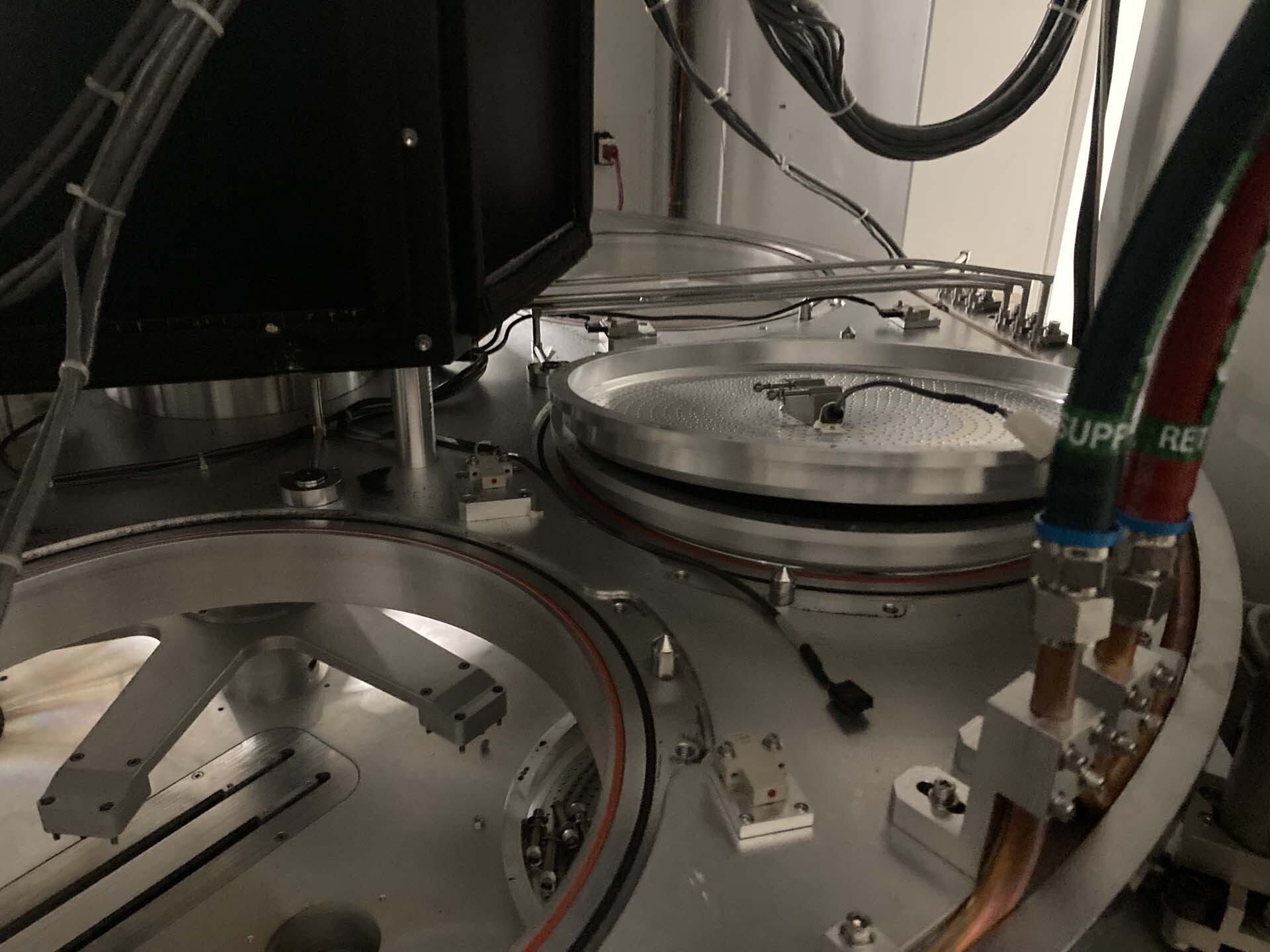

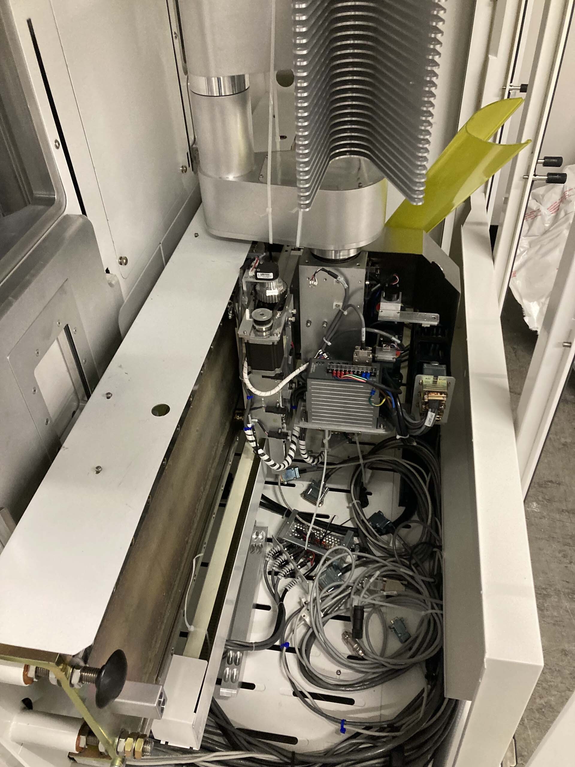

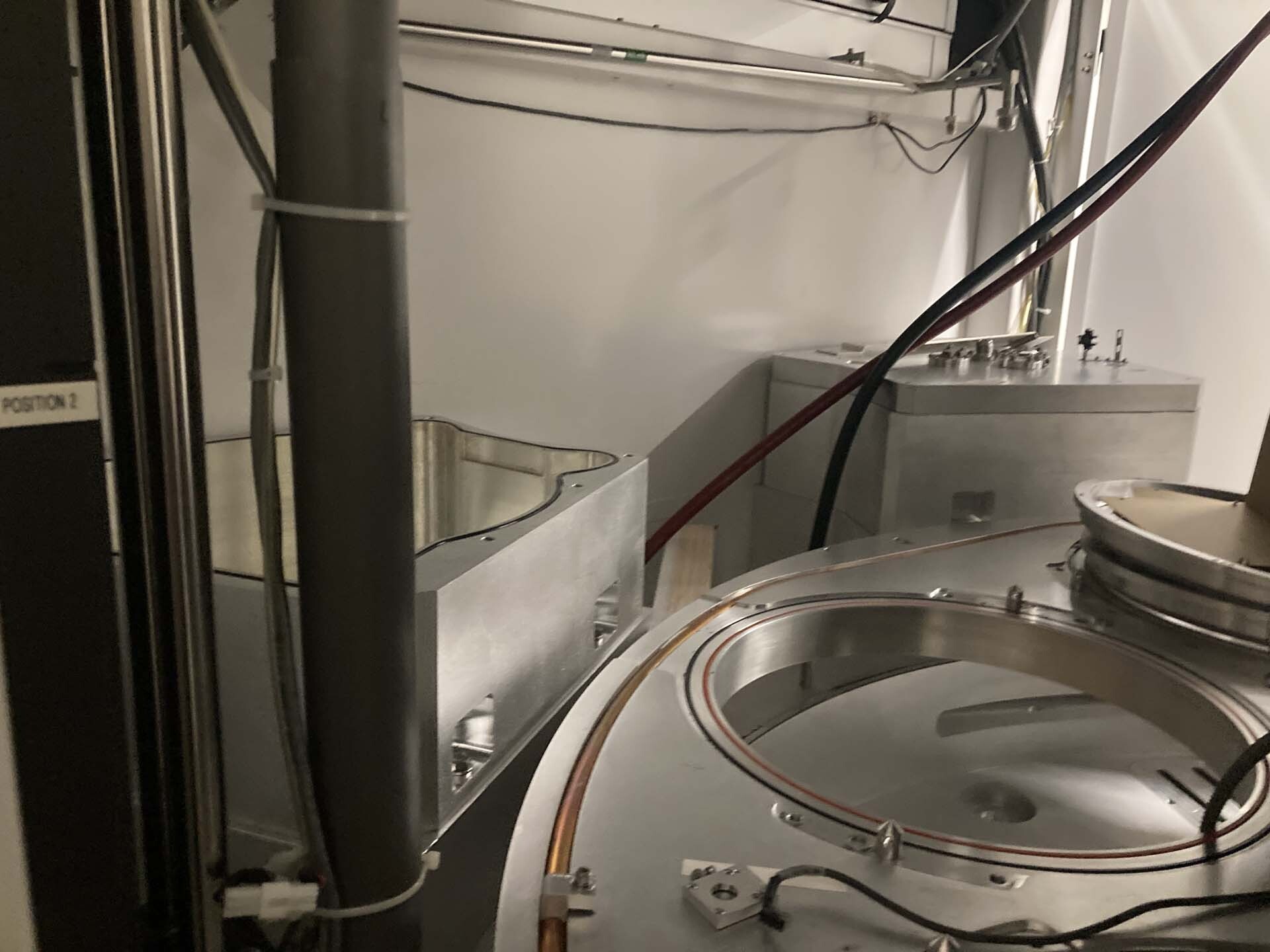

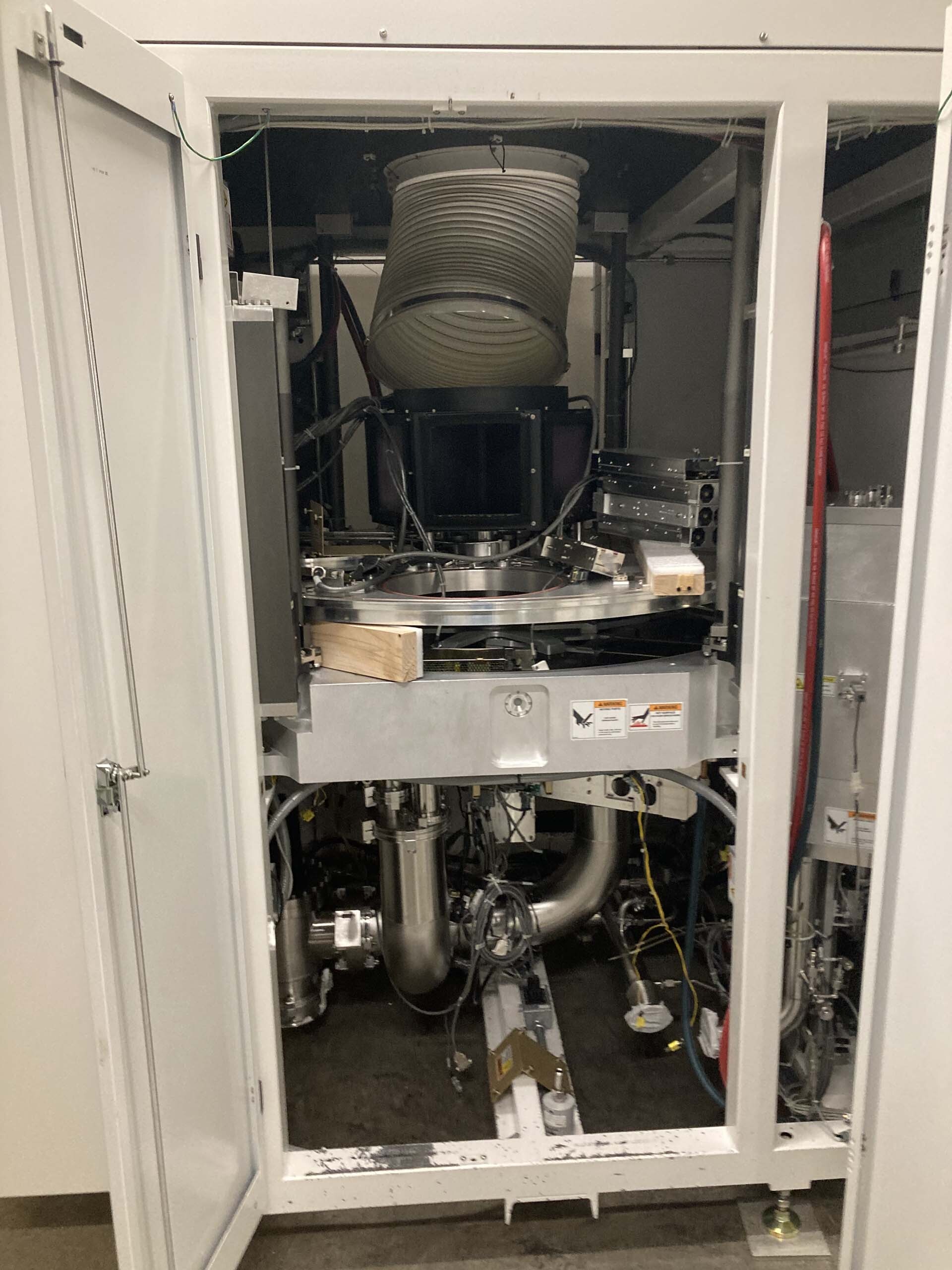

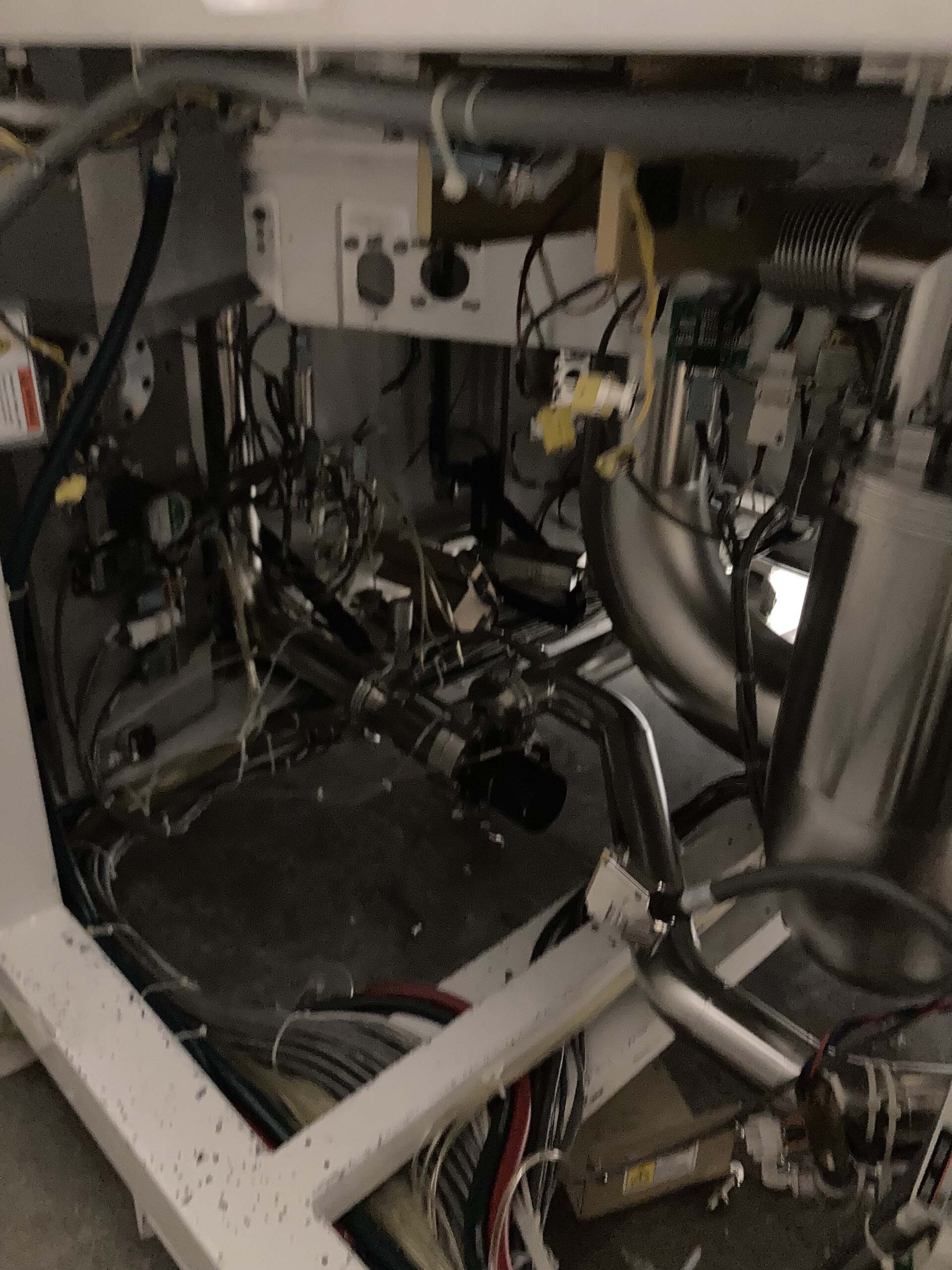

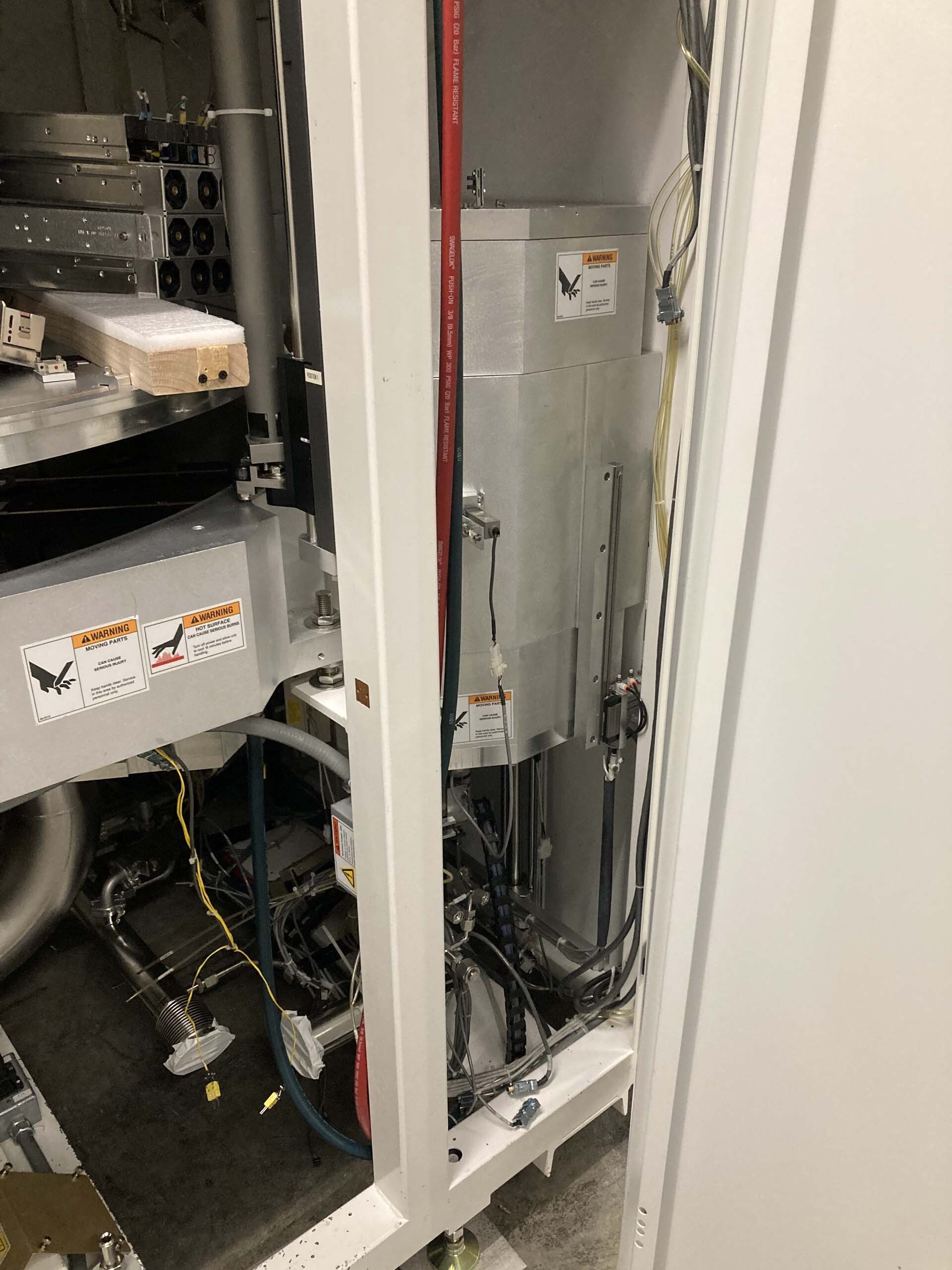

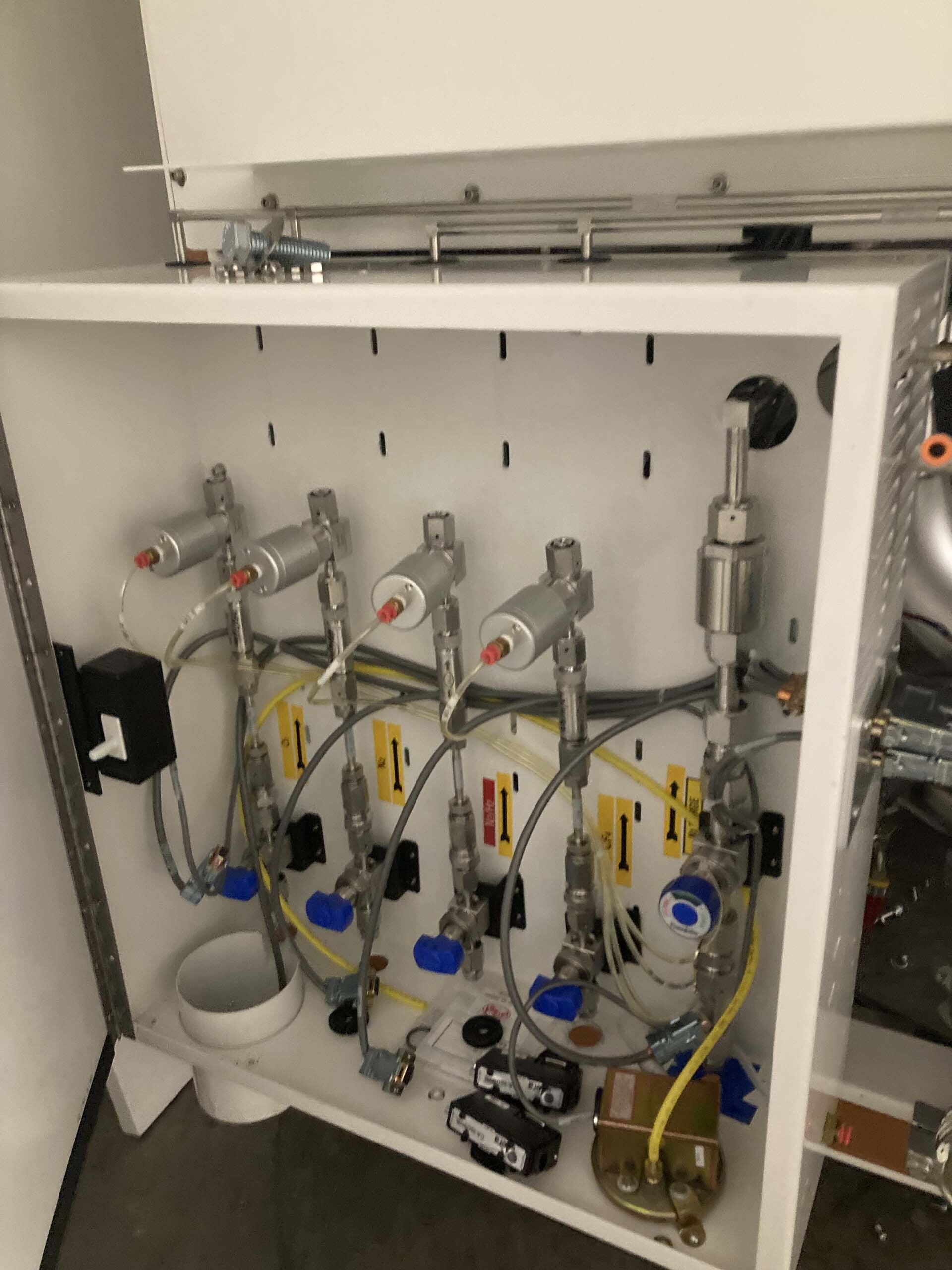

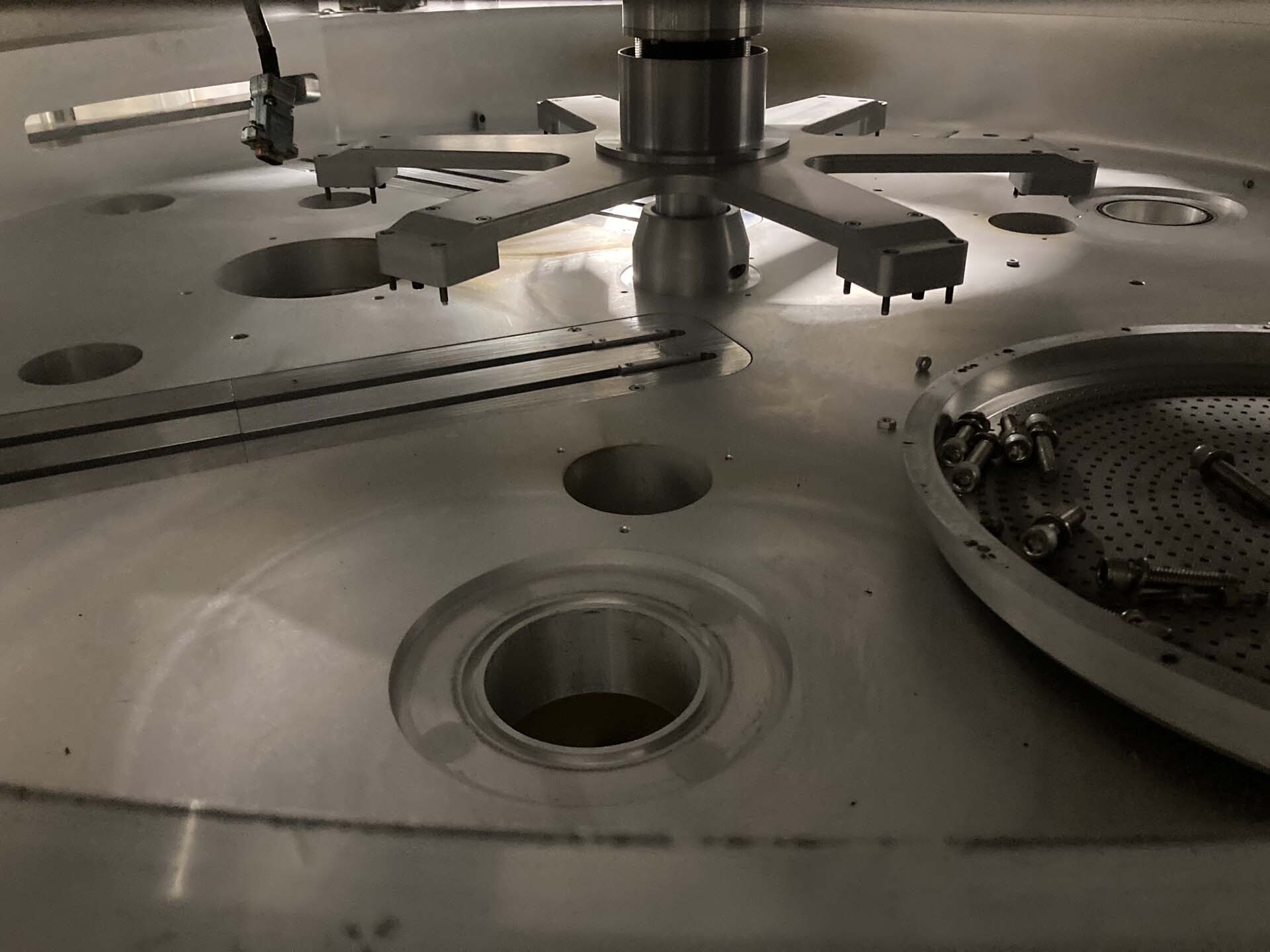

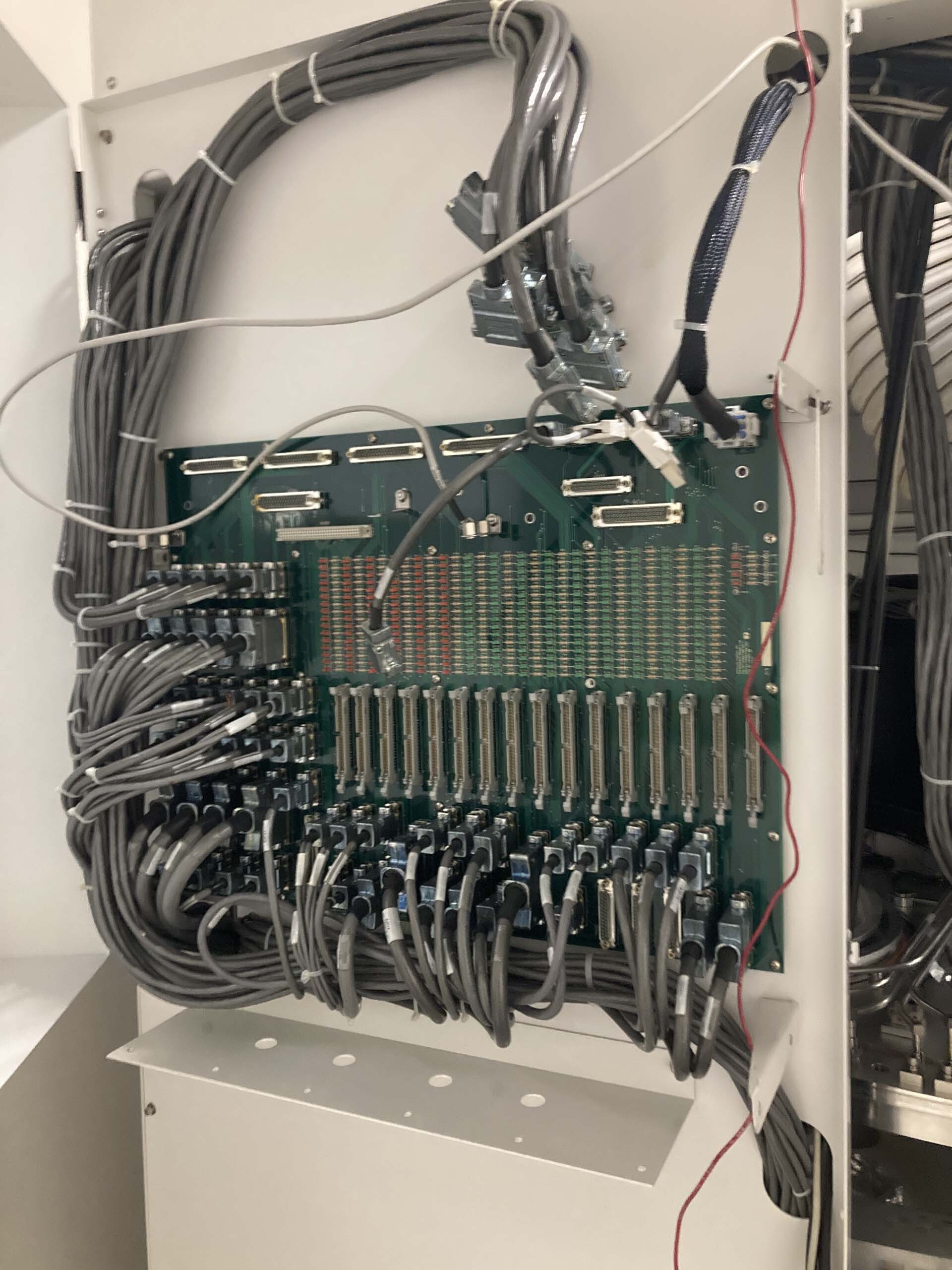

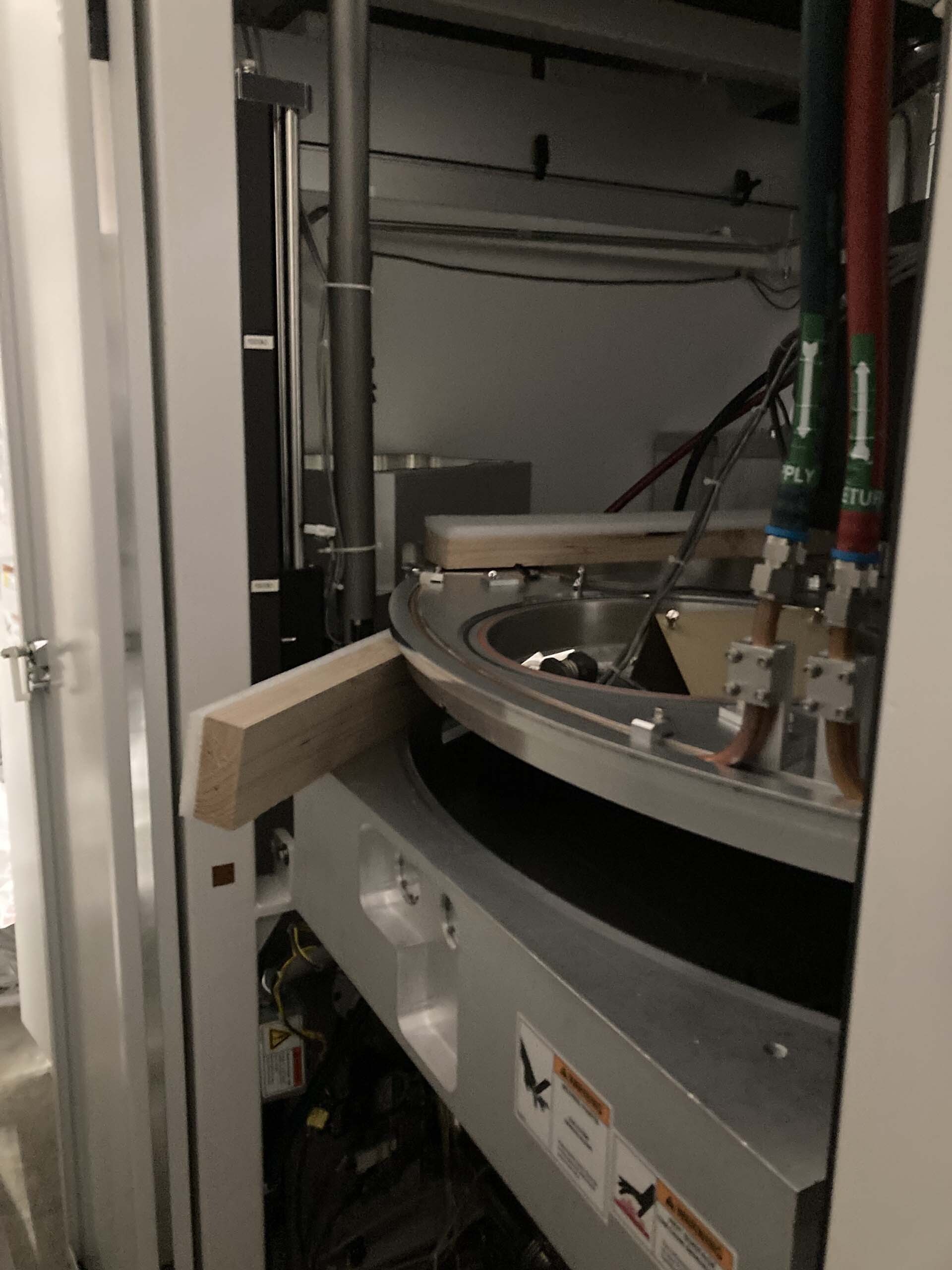


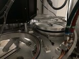
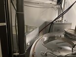
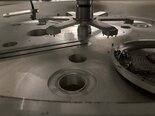
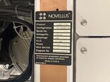
NOVELLUS Gamma 2130 is a high-temperature, plasma-based etcher/ asher developed for wafer-level processing in semiconductor device manufacturing. The equipment is designed to meet the stringent process specifications of the industry and offers superior etch uniformity with unparalleled reproducibility and repeatability. Gamma 2130 provides precise control over etch depth, aspect ratio, and surface roughness, enabling high-performance device structures such as ultra-shallow junctions and gate finger structures. It also provides excellent plasma uniformity and selectivity, ensuring the highest quality structure for each device. The system utilizes inductively coupled plasma (ICP) technology and features a proprietary, wide-beam electron cyclotron resonance (ECR) plasma source that offers superior etch selectivity and etch rate as low as 0.2 nm/min. Its ICP power source provides excellent uniformity of the process across the wafer. The unit includes an Emerson ASC-1000 control machine to ensure tight process control and improve the repeatability and reproducibility of each etch process. NOVELLUS Gamma 2130 features a self-aligning, ceramic narrow-track electrostatic chuck (ESC) to hold the wafer during processing. The ESC provides high uniformity of susceptor chuck temperature and pressure, ensuring uniform etch rate across the entire wafer. Gamma 2130 also features a gas interface panel (GIP) which allows for easy gas loading and unloading, as well as precise control of reactant gas flow rates and mixing. The tool offers flexibility in choice of process gases and their combination, providing a wide variety of process options for various application requirements. The etch process on NOVELLUS Gamma 2130 is optimized with the help of an in-situ ellipsometer for on-the-fly real-time etch endpoint detection. It also offers integrated diagnostic features such as process development, chamber optimization and post-processing analysis. Gamma 2130 can be integrated within a clean room environment easily and offers low operating cost, making it highly efficient and cost-effective. Its superior etch uniformity and selectivity makes it suitable for a wide range of applications such as transistor, capacitor and resistor etch processes.
There are no reviews yet


