Used SEZ / LAM RESEARCH RST 201-8/6 #9394342 for sale
URL successfully copied!
Tap to zoom
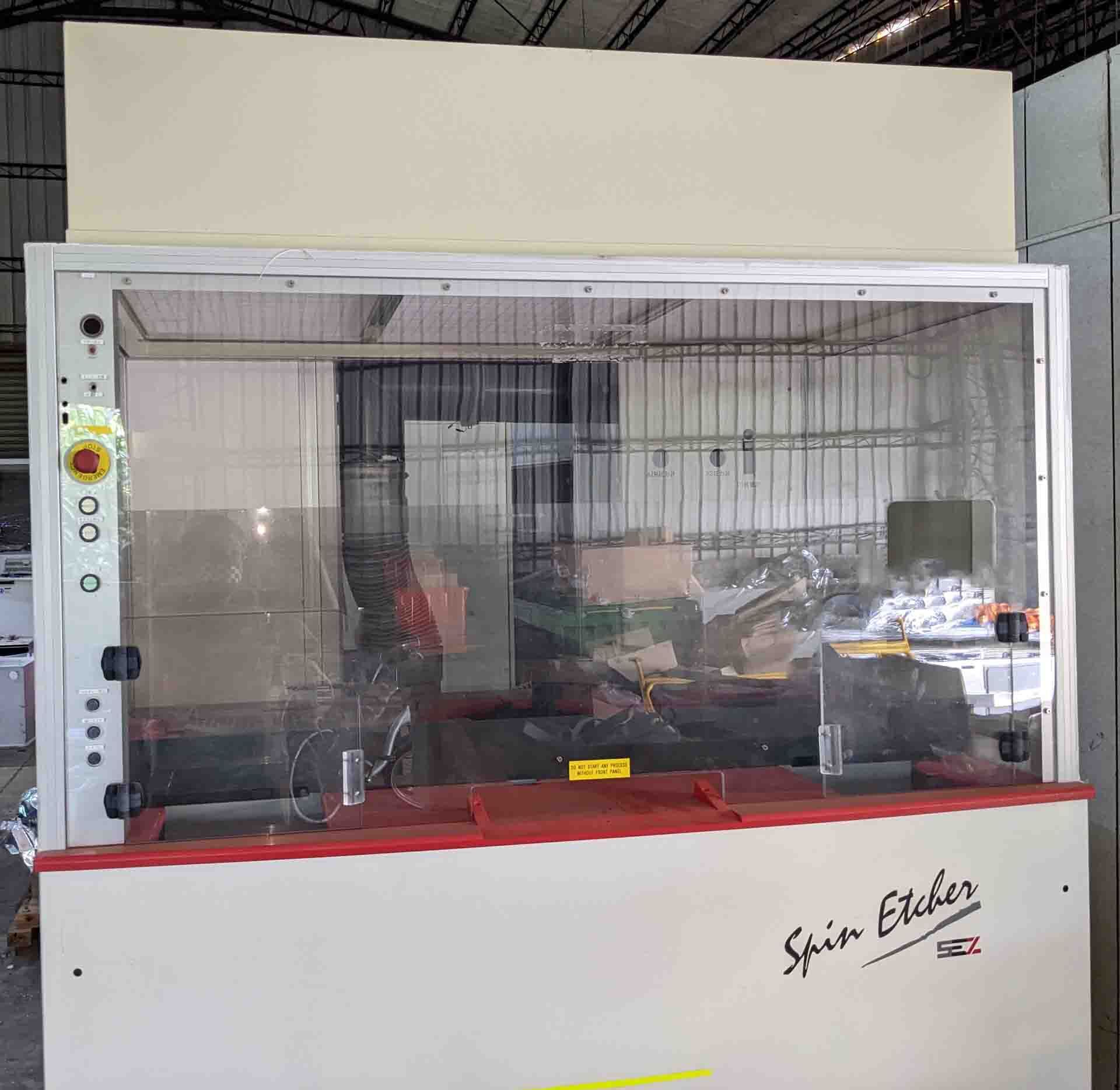

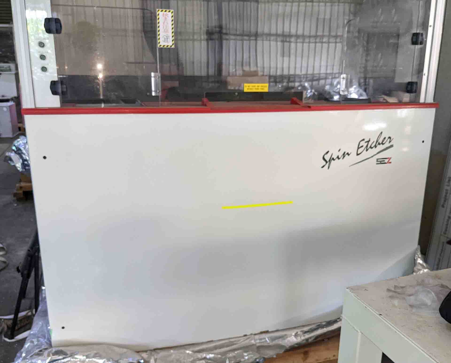

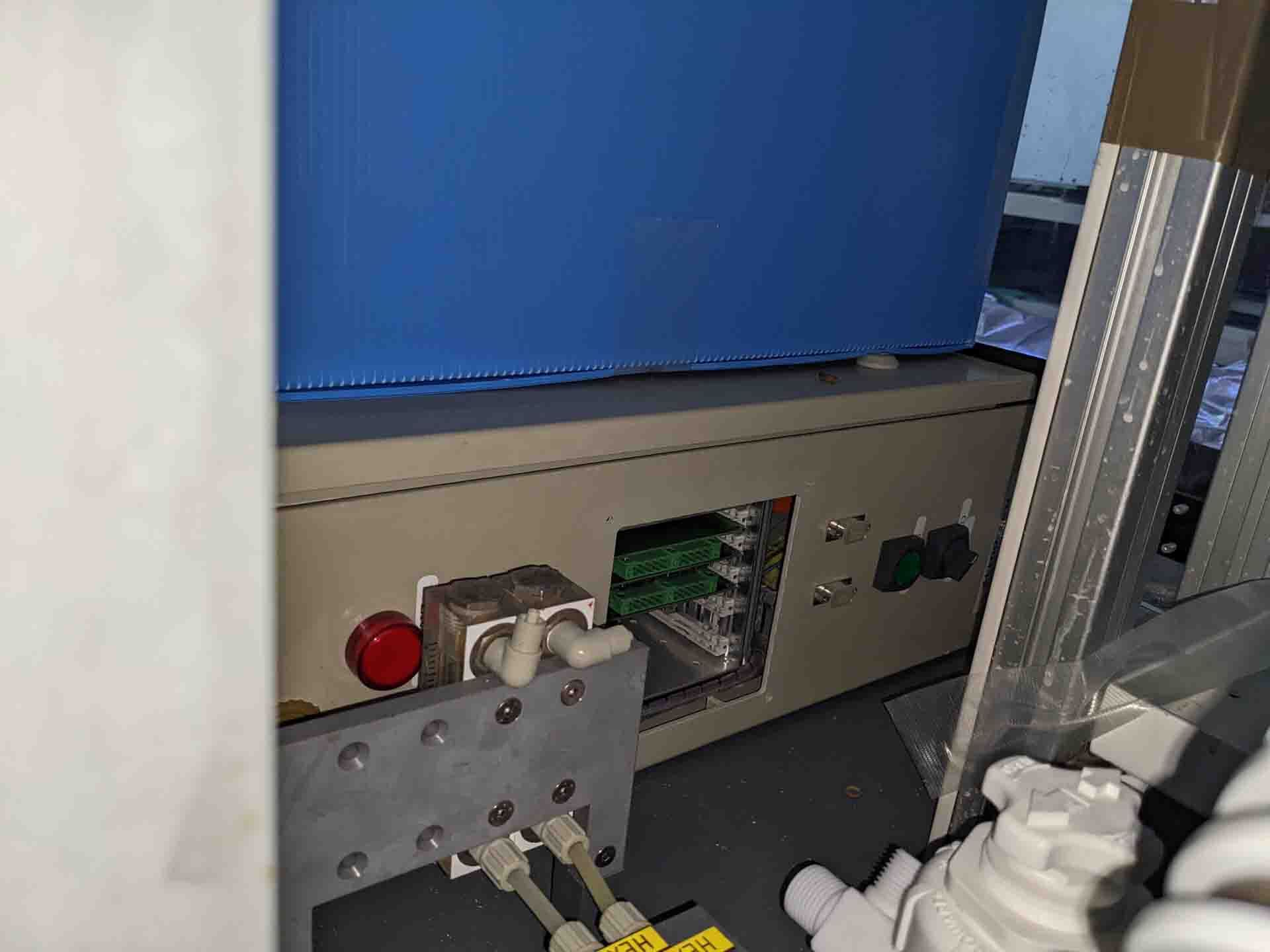

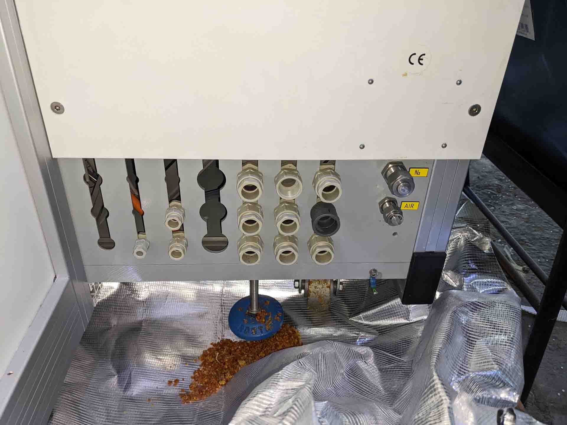

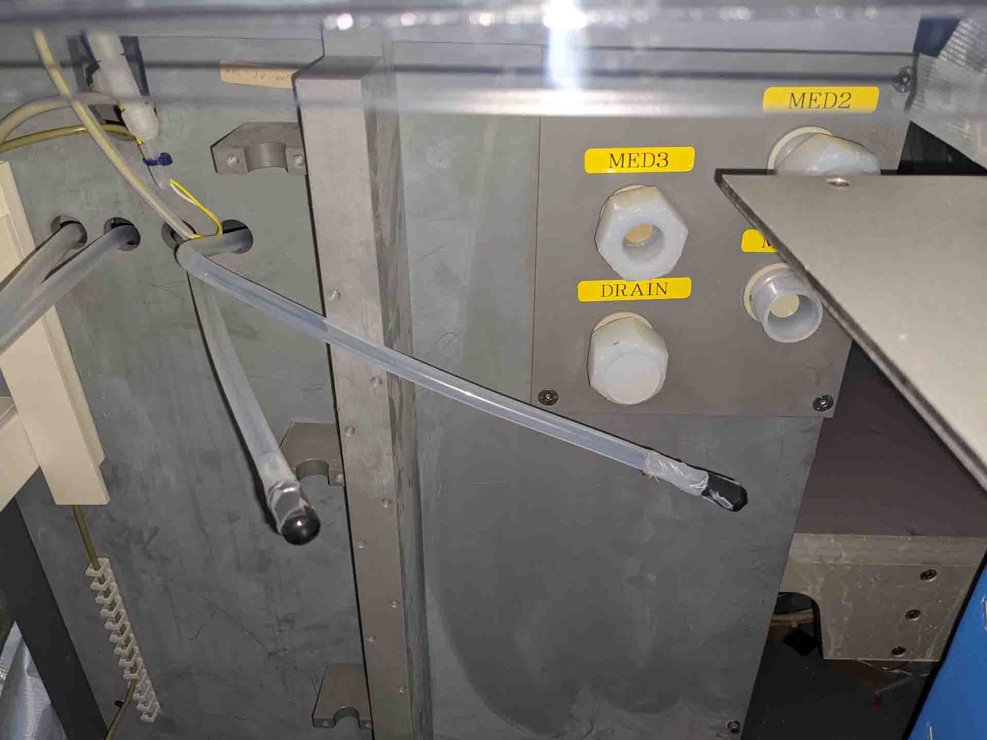

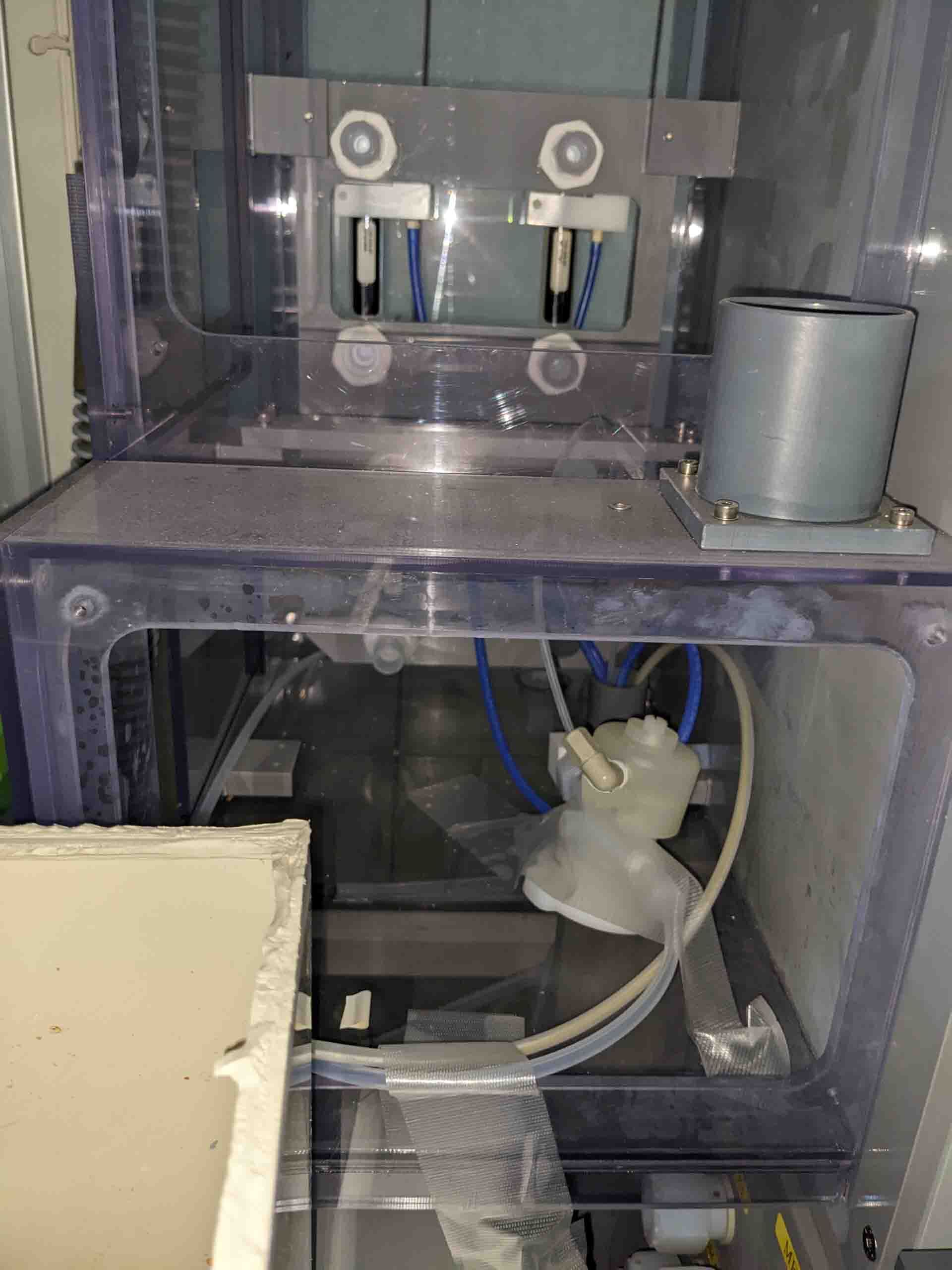

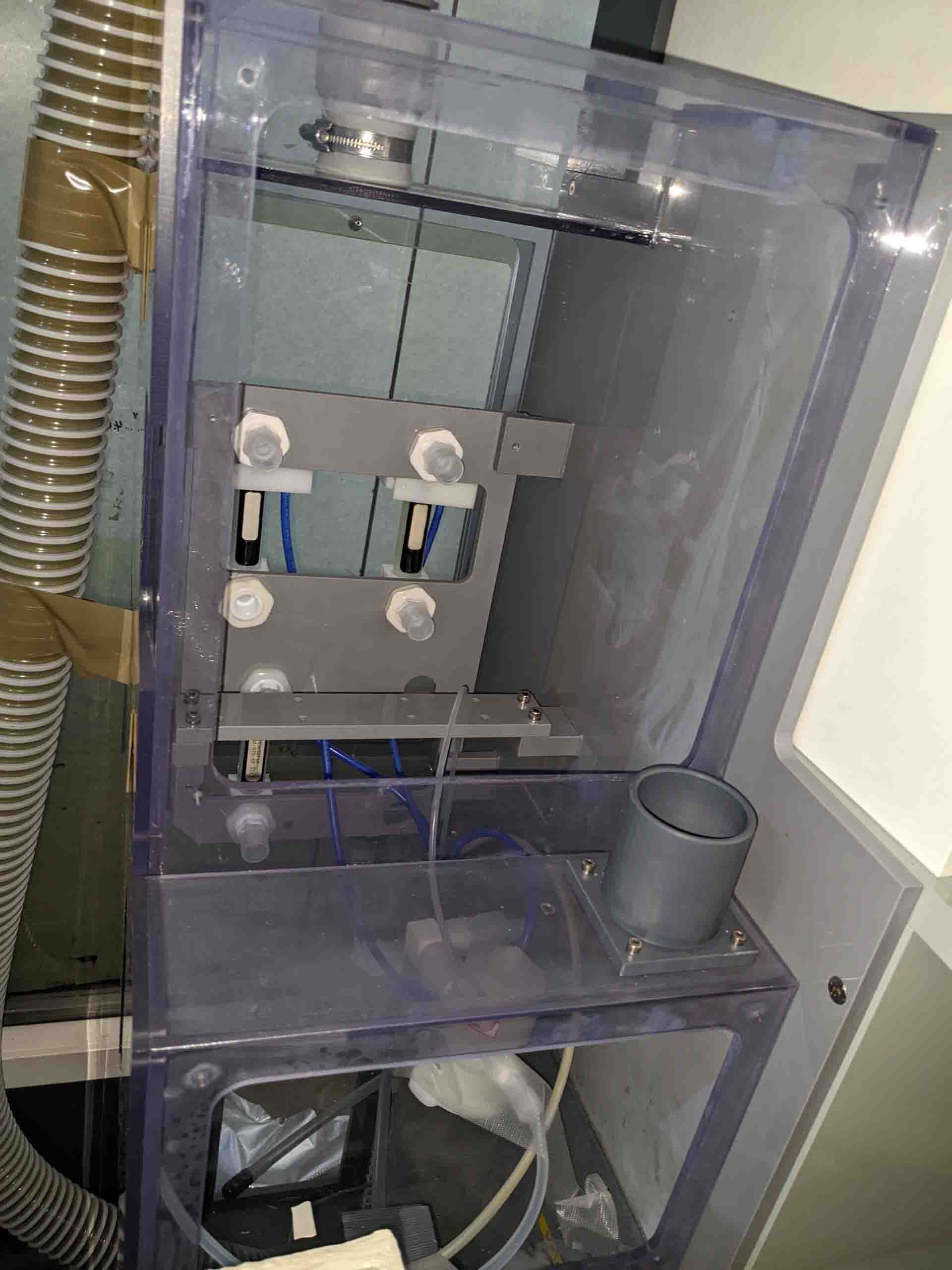

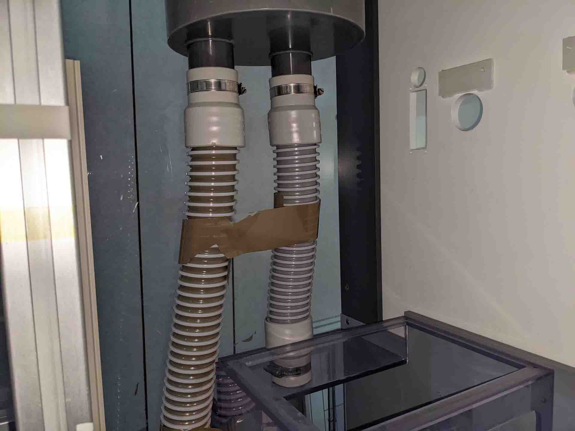


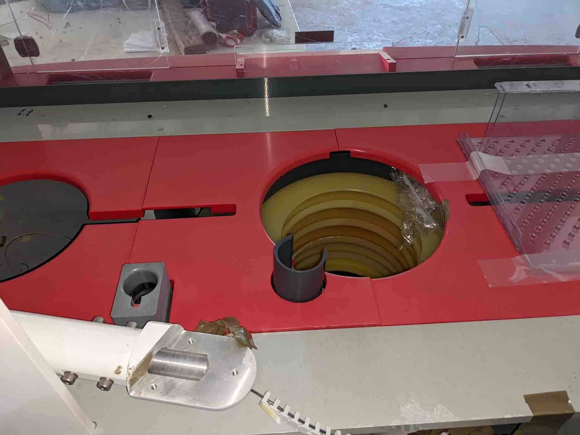

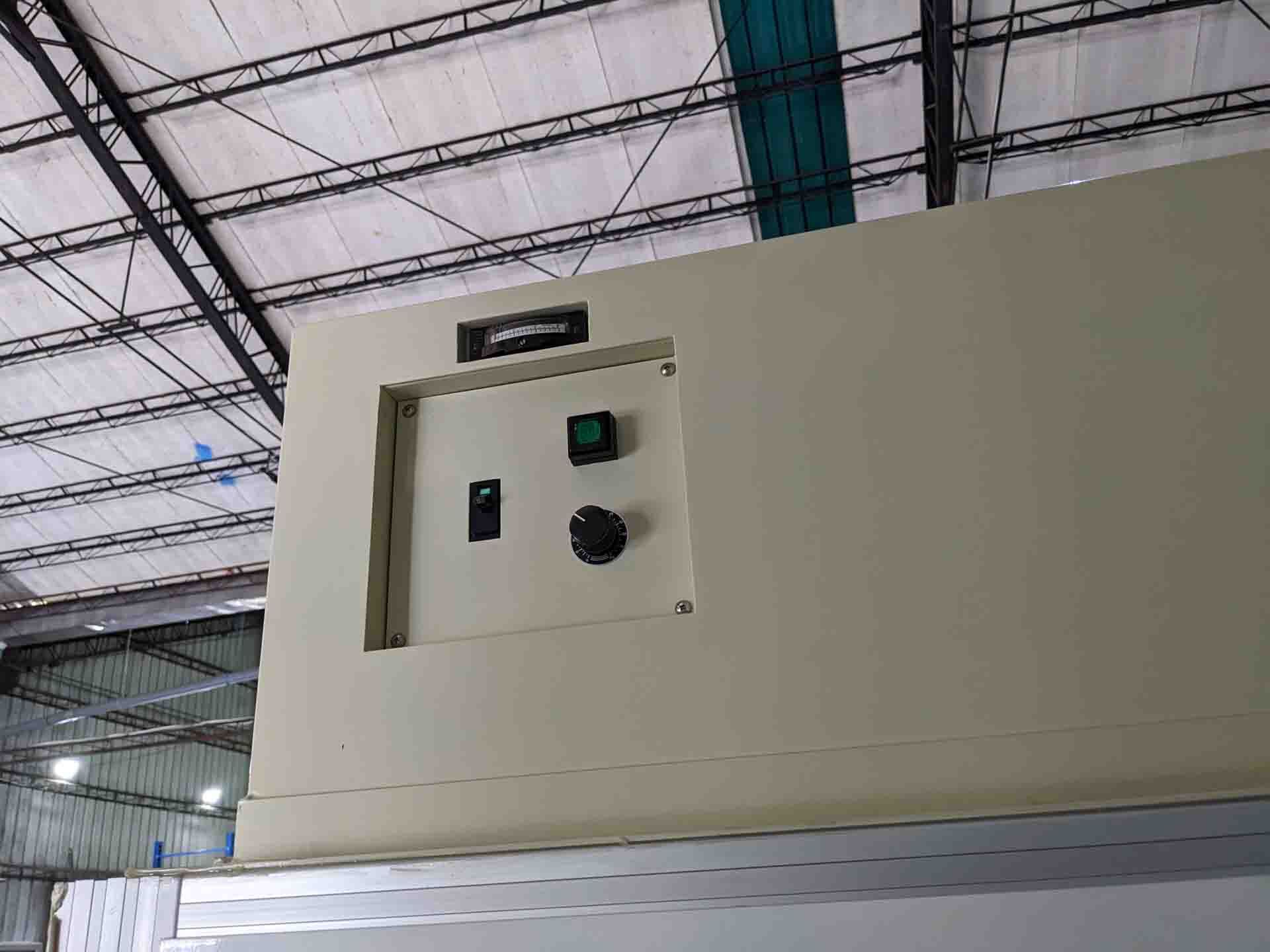


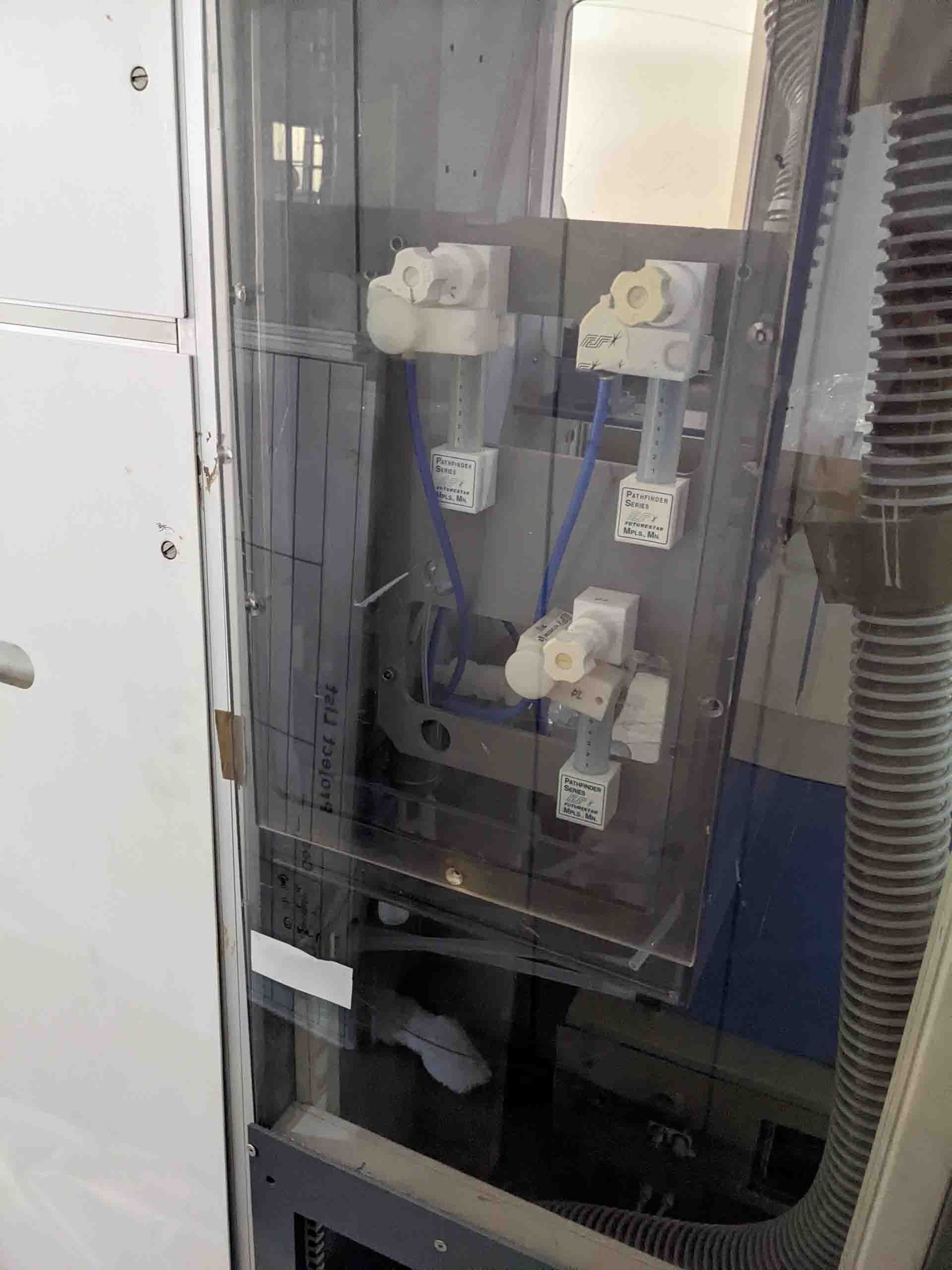

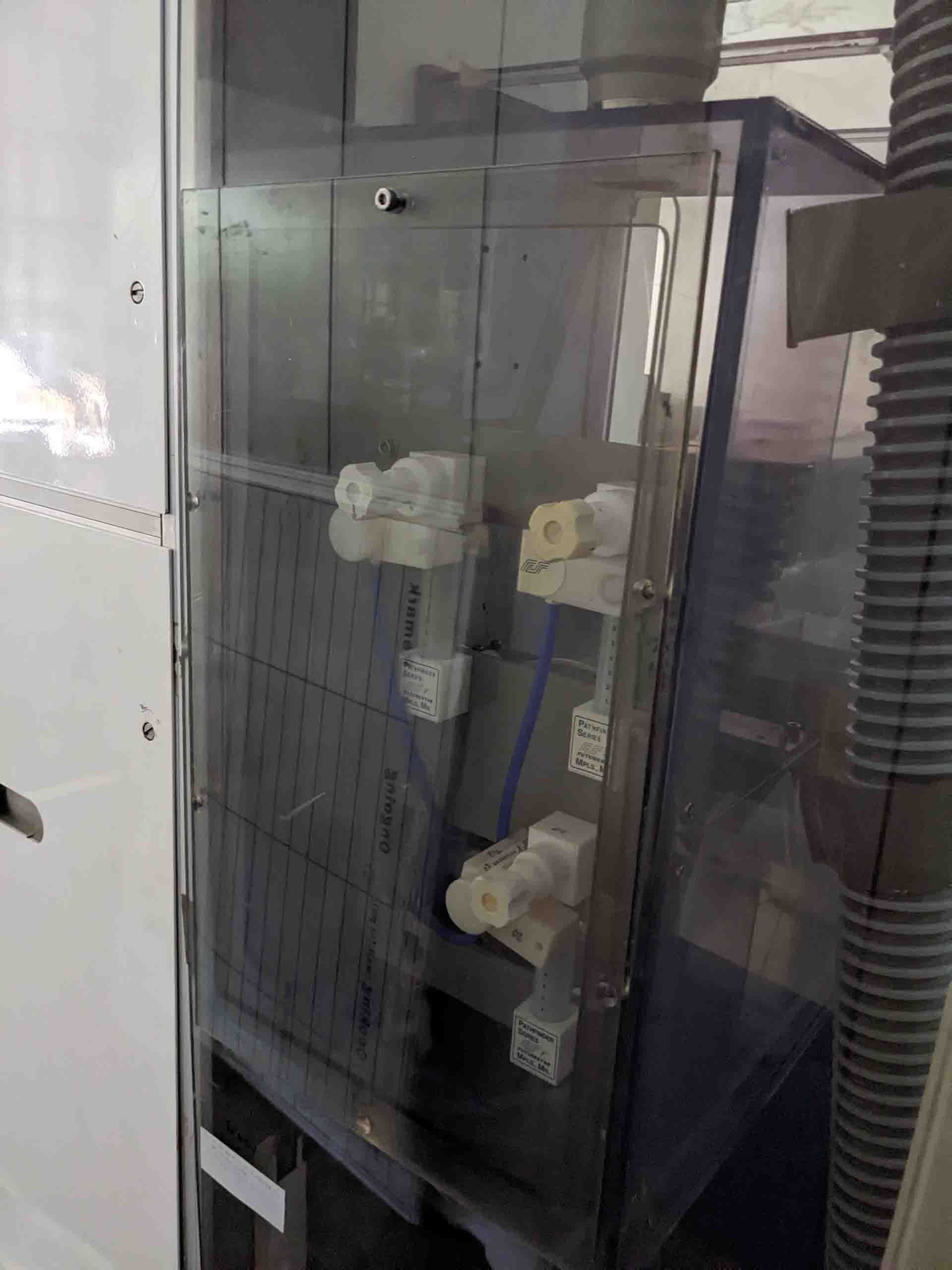

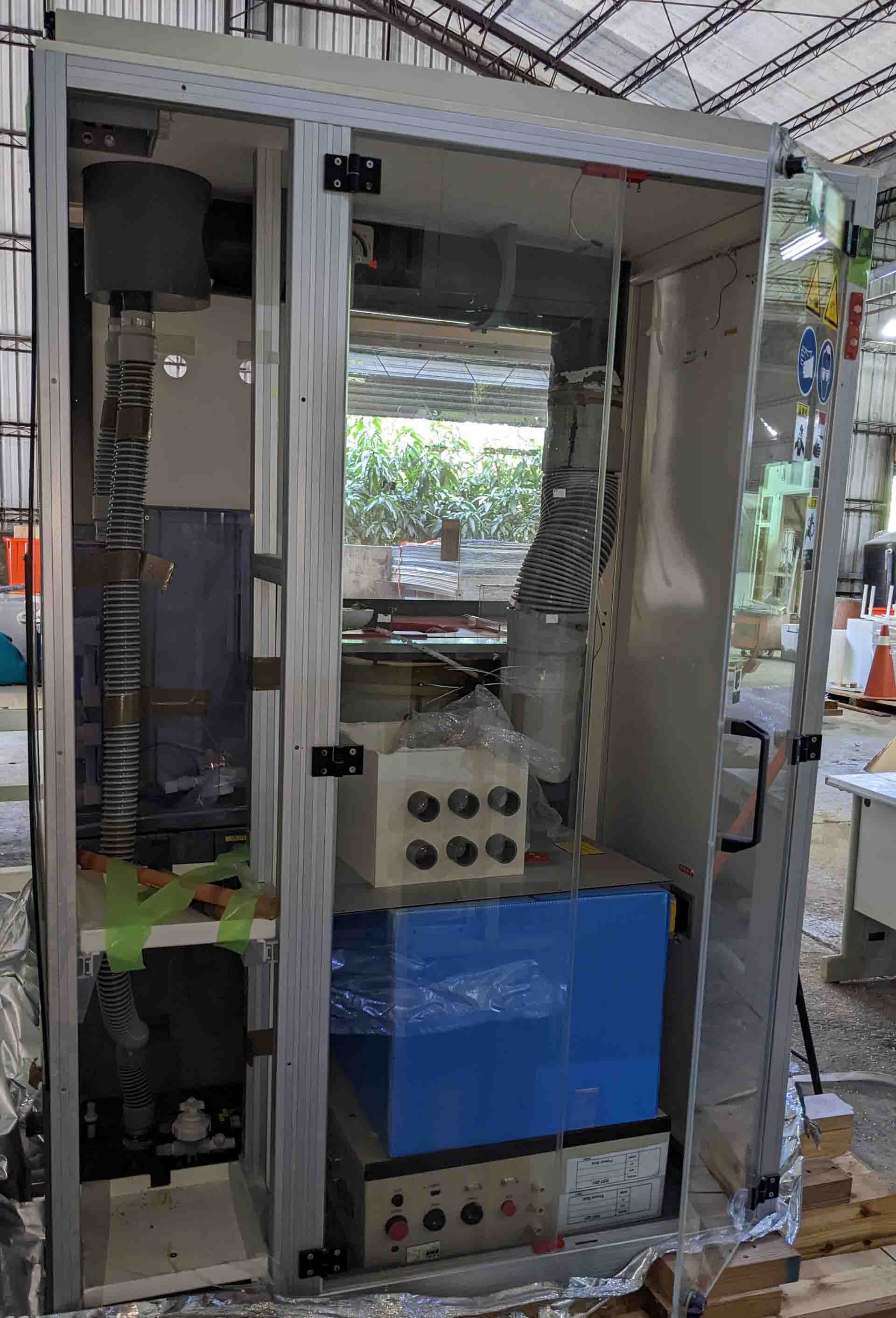


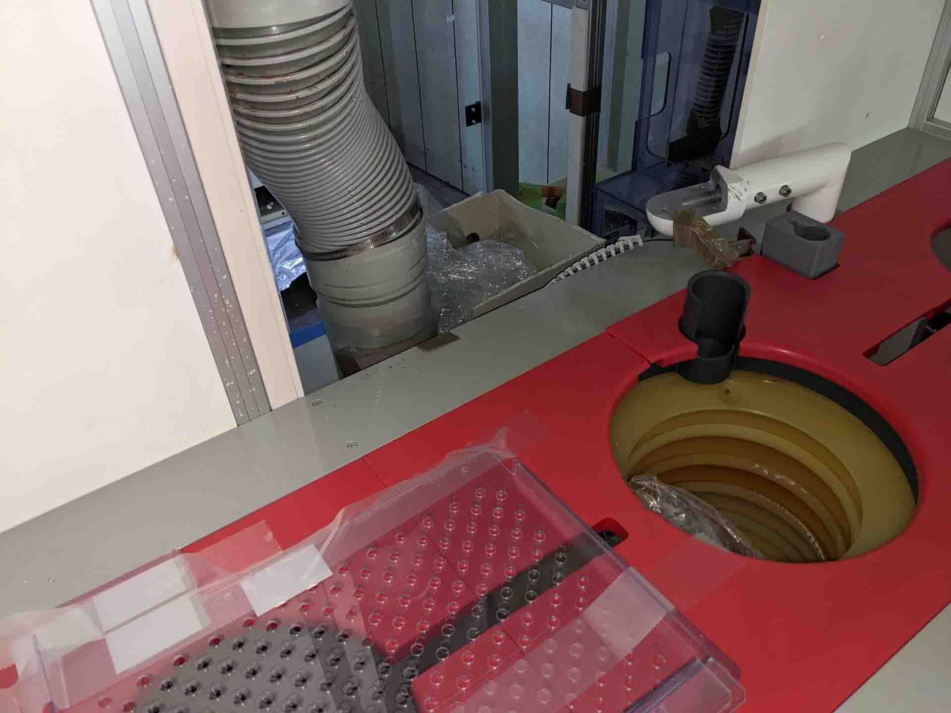

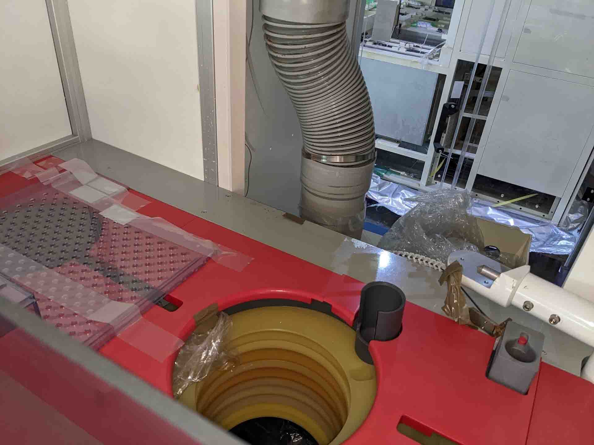

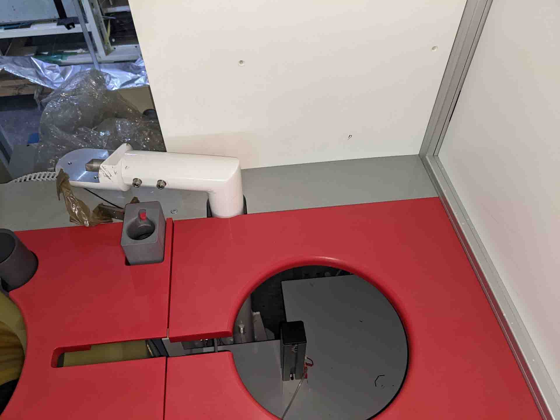




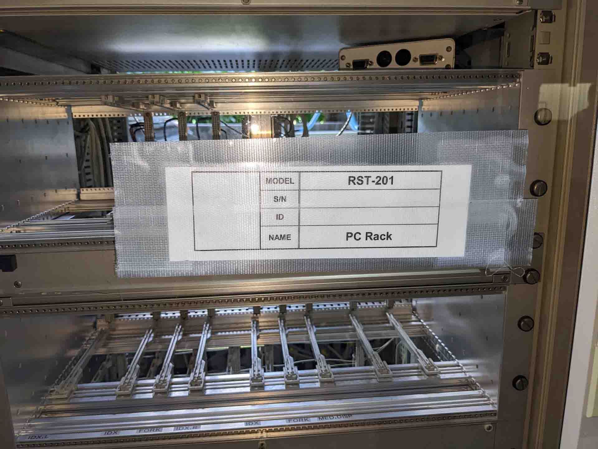

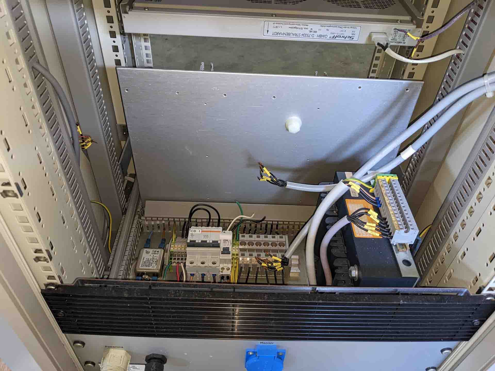

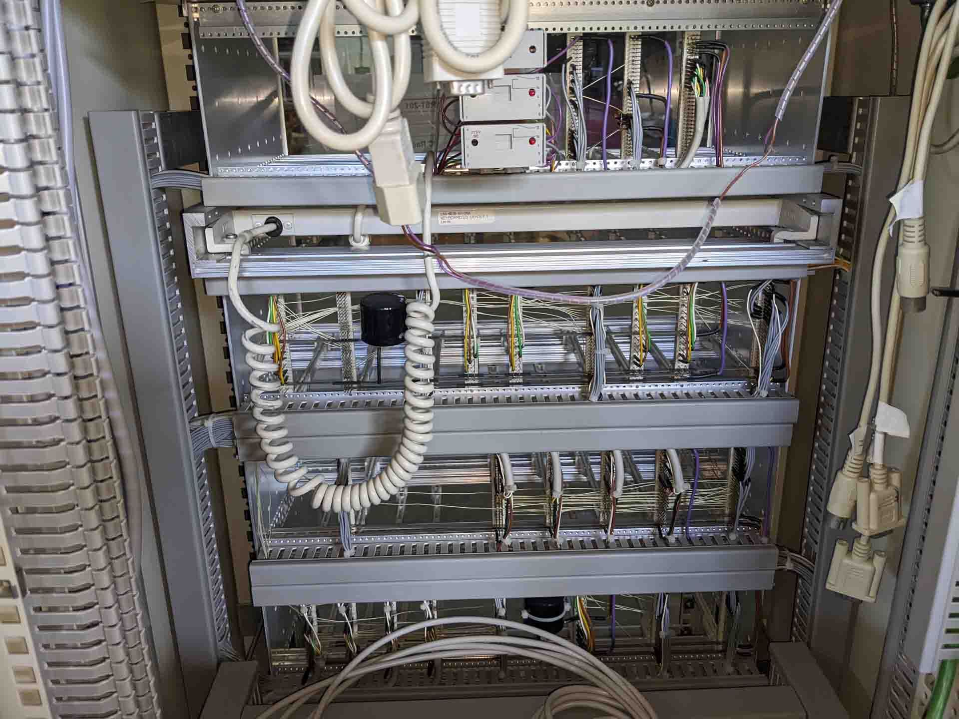


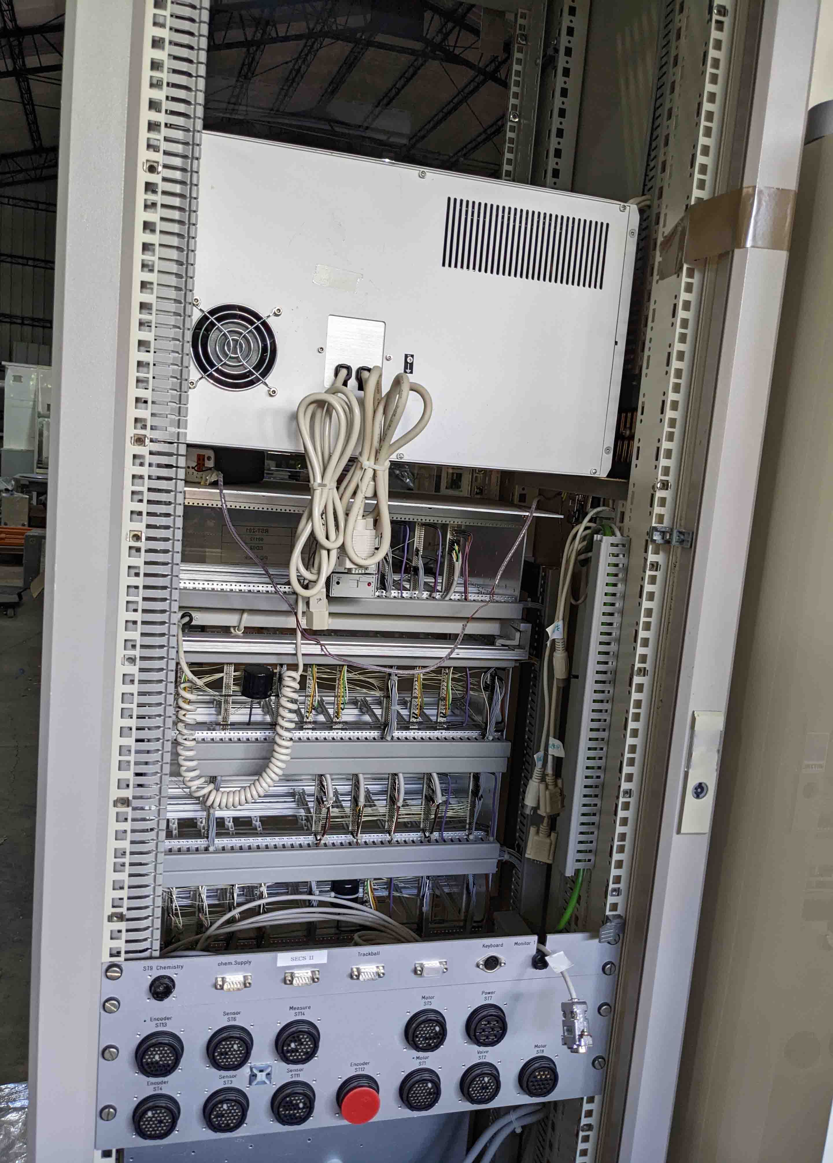


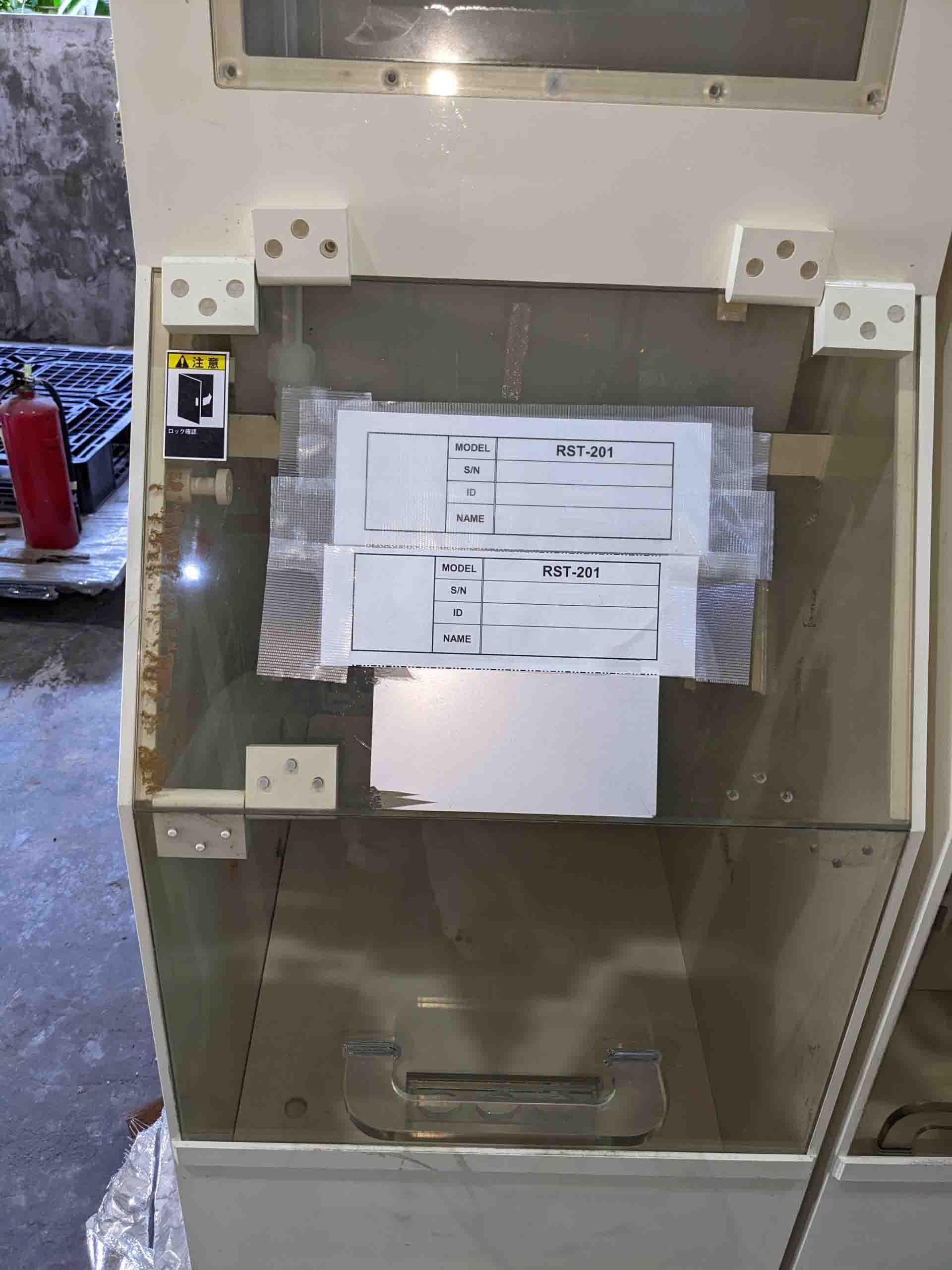

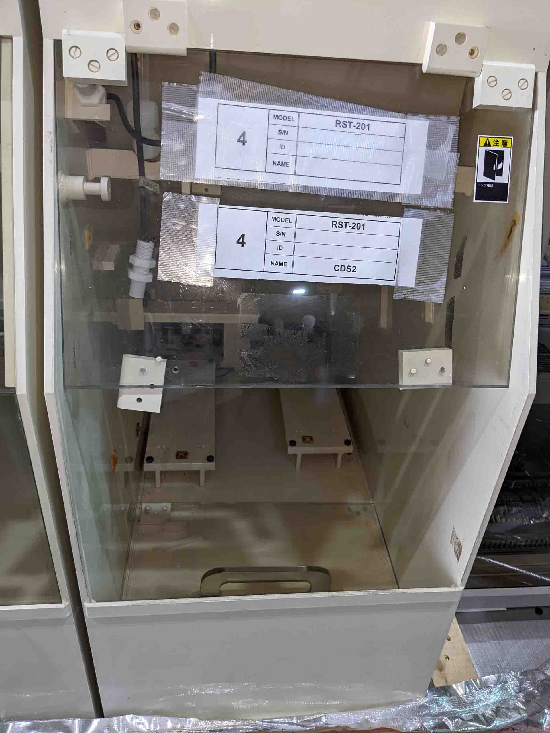

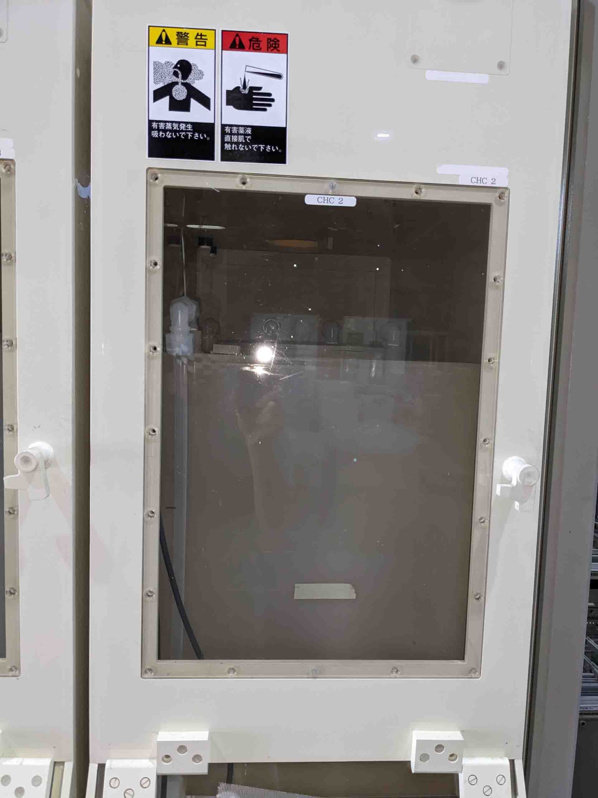

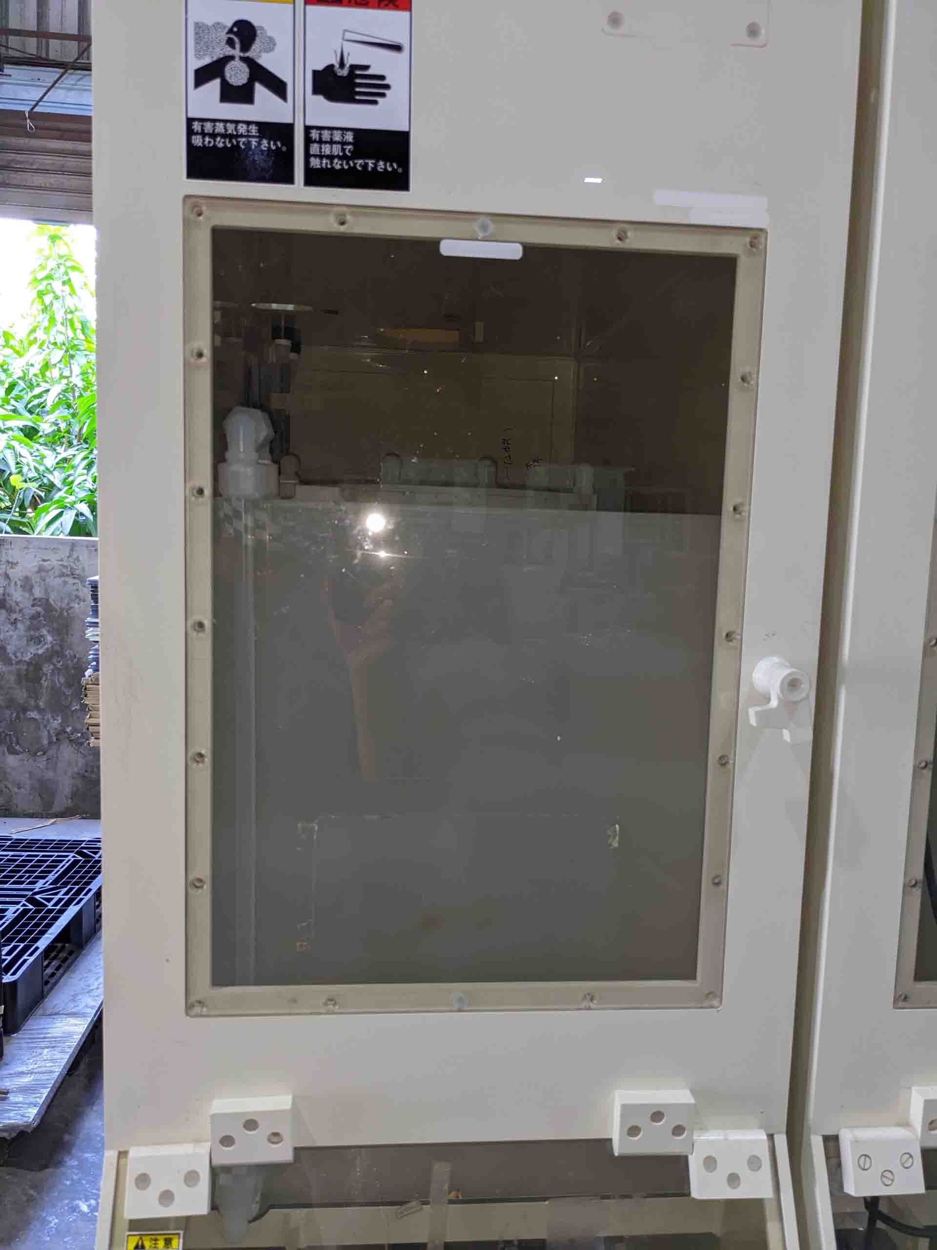

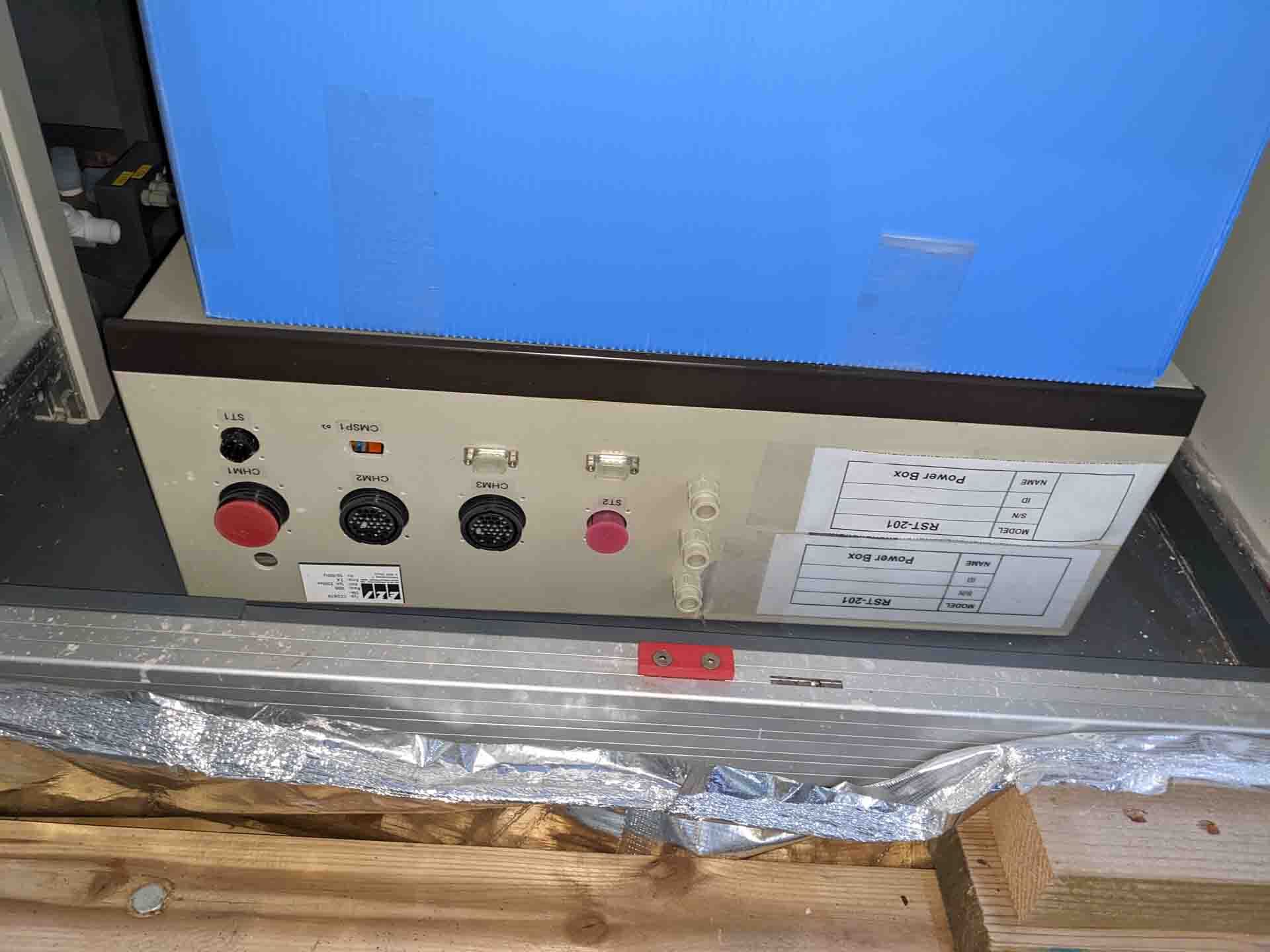

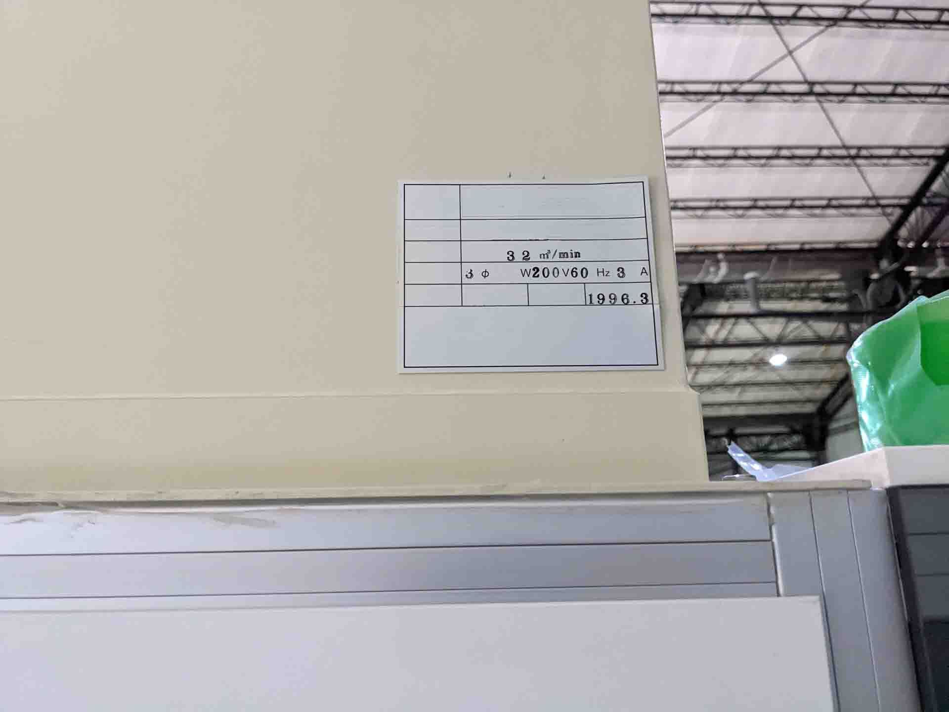


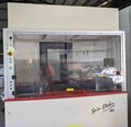
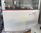
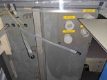
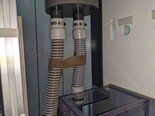
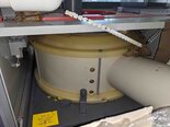
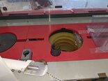
SEZ RST 201-8/6 is an etcher/asher, used in the production of semiconductor devices. It is manufactured by LAM RESEARCH, a multinational corporation specializing in the production and distribution of etch/ashers and other semiconductor equipment. This model is designed for the removal of thin layers of material from the surface of semiconductor wafers, such as patterned sapphire substrates. This is a wet etch equipment, which utilizes chemical solutions to etch the wafers to the desired shape and size. SEZ / LAM RESEARCH RST 201-8/6 has a fully automated computer control system, featuring an LCD touch screen interface and advanced software for setting parameters and controlling the etching process. It can be programmed for etching at a wide range of temperatures, and the rate of etching can be adjusted while the process is underway. The unit includes a backside scrubber for cleaning the wafers before etching, and a gas distributor to control the production of chlorine for additional etching. The etching itself is performed in a circular chamber, in which the wafer is rotated during etching. The chamber itself is composed of two rotating lids and the wafers are rotated around a central shaft. Laser beam welding is used to turn off the chamber for maintenance work. Additionally, the RST 201-8/6 is equipped with sensors to detect any leaks or accidents that might occur. SEZ RST 201-8/6 is capable of etching wafers up to 8 inches in diameter, with a throughput of up to 8 wafers at a time. It has a normalized etch rate of 6nm /min, though this rate can be increased to as much as 30nm/min depending on the material being etched and the power output of the laser. Additionally, the machine is capable of handling both small-scale test runs and large-scale production runs. LAM RESEARCH RST 201-8/6 can be used in a wide variety of applications, from patterning substrates with a minimum line width of 0.1 micron to creating complex 3D shapes. It is a reliable and cost-effective tool which can be used in a wide range of semiconductor manufacturing processes.
There are no reviews yet
