Used SEZ / LAM RESEARCH SP 200 #293816234 for sale
URL successfully copied!
Tap to zoom
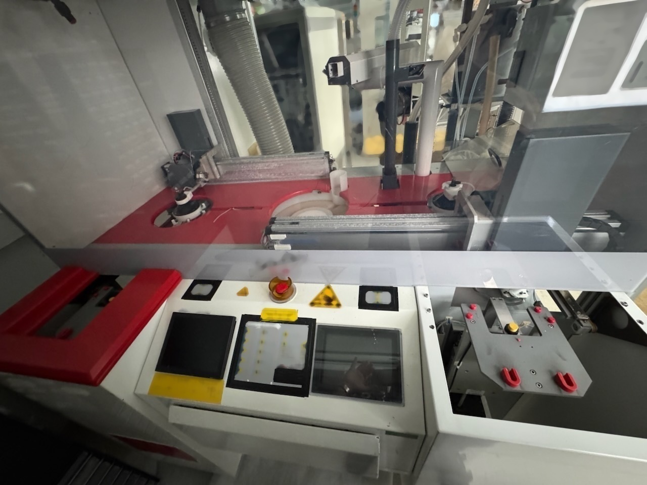

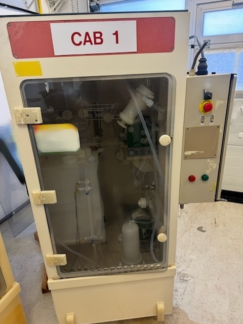
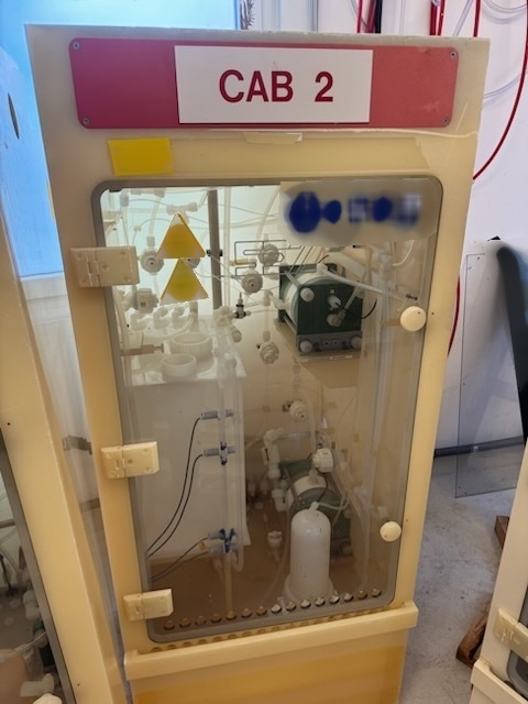
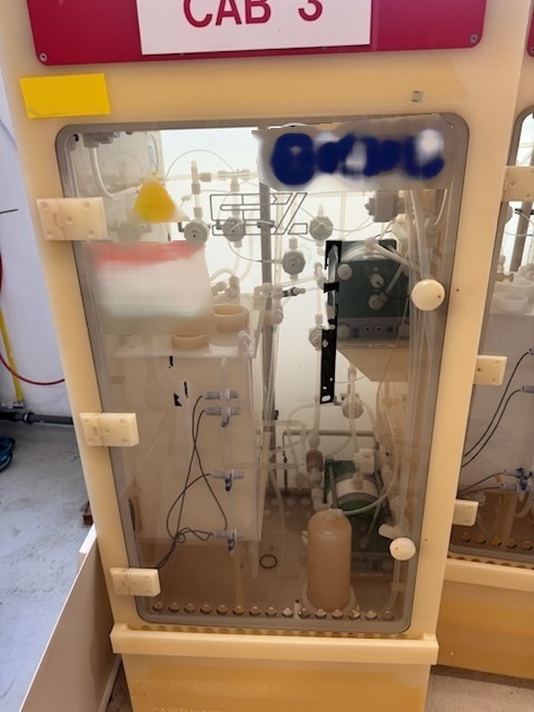
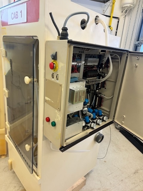
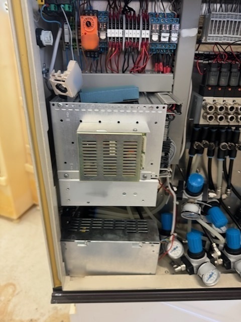
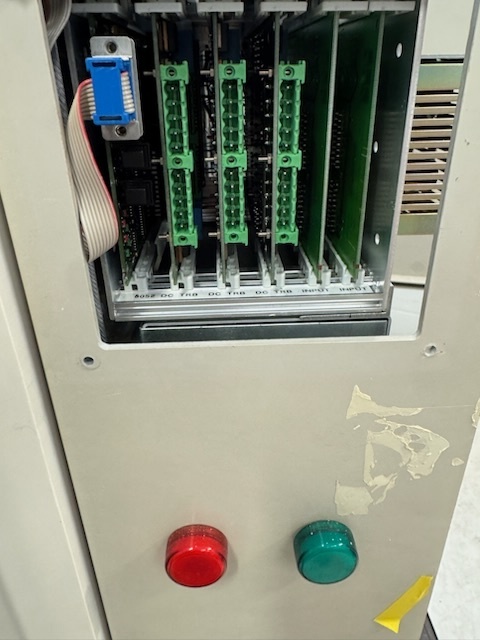
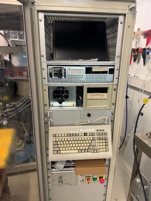
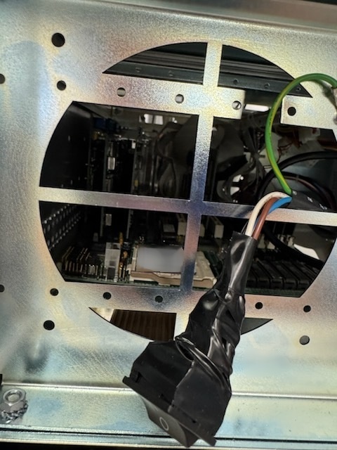
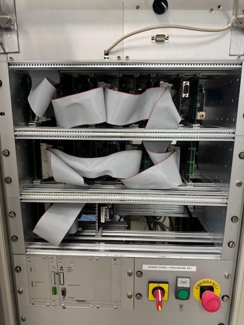
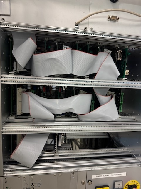
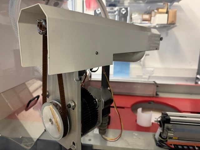
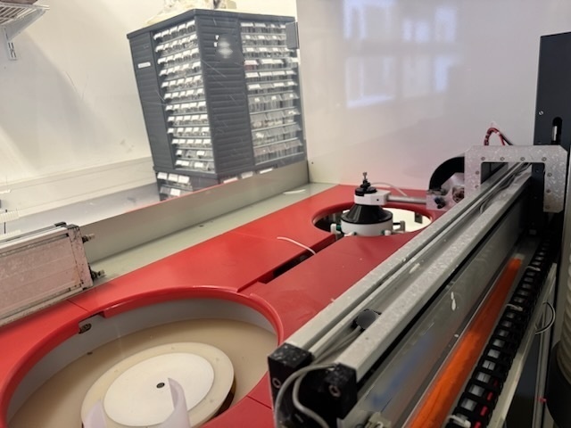
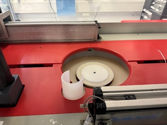
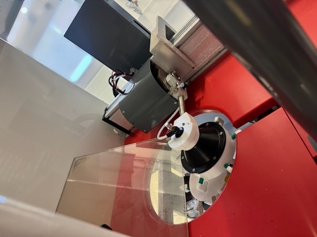
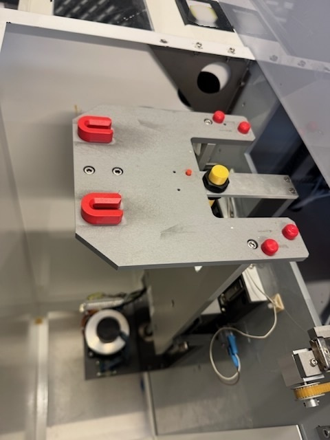
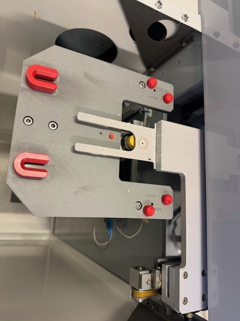
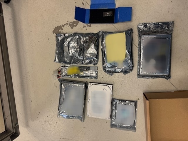
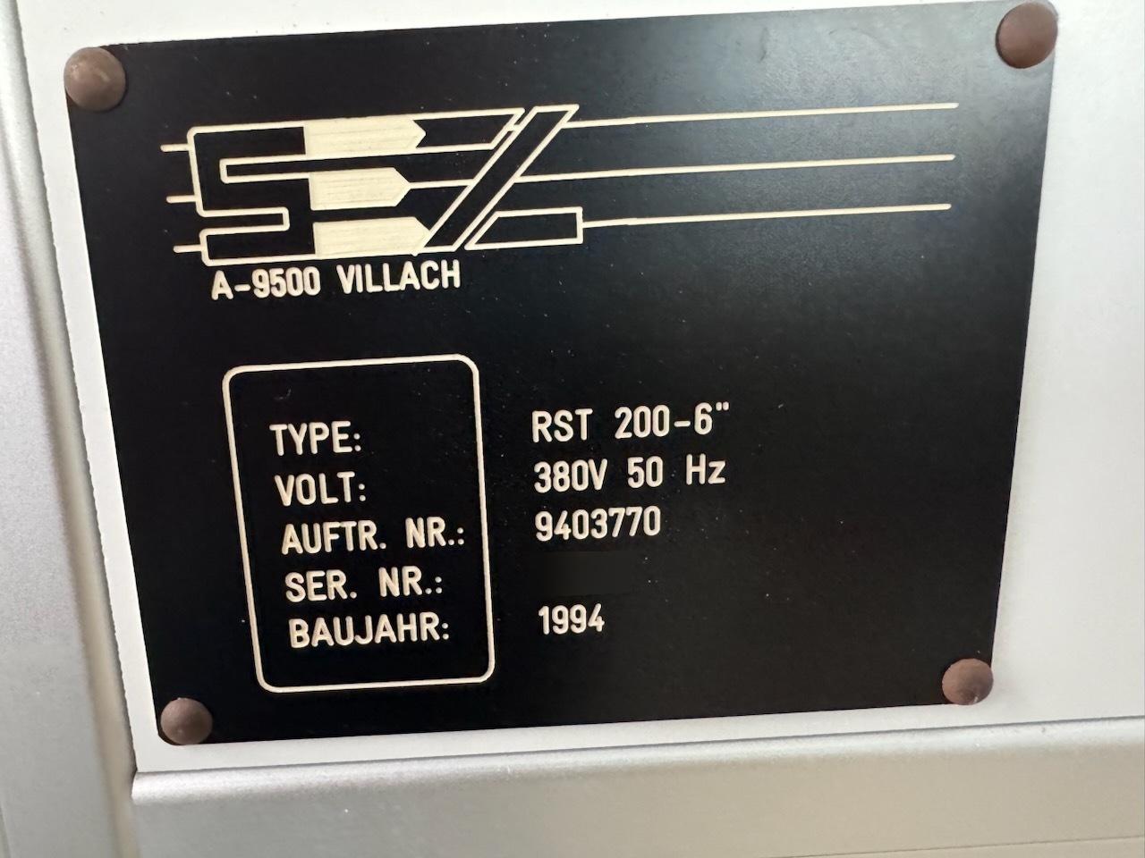
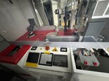
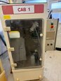
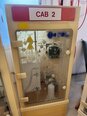
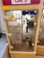
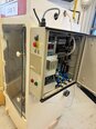
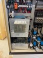
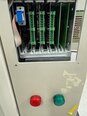
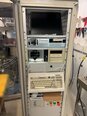
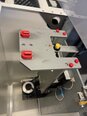
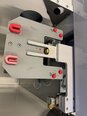
**Introduction** SEZ / LAM RESEARCH SP 200 is a highly advanced etcher/asher equipment, designed for semiconductor manufacturing processes in the microelectronics industry. This cutting-edge equipment integrates superior process control capabilities with precision plasma etching and ashing technologies, enabling the fabrication of high-performance semiconductor devices with exceptional quality and reliability. **Key Features** SEZ SP 200 boasts a plethora of innovative features that set it apart from conventional etchers/ashers. Here are some of the key highlights: 1. **Advanced Process Control**: LAM RESEARCH SP 200 is equipped with advanced process control algorithms that ensure precise control over etch rates, selectivity, and uniformity. This leads to improved process stability and repeatability, resulting in superior device performance and yield. 2. **Multi-Process Capability**: The flexibility of SP 200 allows it to perform a wide range of processes, including etching, ashing, descum, and resist stripping. This versatility makes it a cost-effective solution for various semiconductor fabrication steps. 3. **High Throughput**: SEZ / LAM RESEARCH SP 200's high-speed processing capabilities enable efficient batch processing of wafers, leading to increased productivity and reduced manufacturing cycle times. 4. **Superior Etching Performance**: SEZ SP 200 utilizes advanced plasma etching techniques to achieve high aspect ratio etching with high selectivity and minimal sidewall damage. This results in precise pattern transfer and superior device performance. 5. **Enhanced Safety Features**: LAM RESEARCH SP 200 is equipped with a comprehensive range of safety features, including gas leak detection systems, emergency shutdown mechanisms, and interlock systems to ensure operator safety and equipment protection. 6. **Efficient Gas Delivery System**: SP 200 features a sophisticated gas delivery unit that enables precise control over process gases, ensuring optimal process conditions and consistent results. 7. **User-Friendly Interface**: SEZ / LAM RESEARCH SP 200 is designed with a user-friendly interface that simplifies operation and facilitates quick setup and programming. Intuitive software controls allow for easy parameter adjustments and real-time monitoring of process parameters. **Applications** SEZ SP 200 finds extensive applications in the semiconductor industry for various processes, including: 1. **Photoresist Stripping**: LAM RESEARCH SP 200 is commonly used for ashing and stripping photoresist layers from semiconductor wafers, ensuring clean substrate surfaces for subsequent processing steps. 2. **Descum**: SP 200 effectively removes residue and contaminants from wafers through descum processes, improving device reliability and performance. 3. **Etch and Pattern Transfer**: SEZ / LAM RESEARCH SP 200 facilitates high-precision etching and pattern transfer processes essential for creating intricate device structures and circuitry on semiconductor wafers. 4. **Device Testing and Failure Analysis**: SEZ SP 200 enables device testing and failure analysis by providing precise etching capabilities for revealing internal structures and defects within semiconductor devices. **Conclusion** In conclusion, LAM RESEARCH SP 200 is a state-of-the-art etcher/asher machine that delivers unmatched performance, versatility, and reliability for semiconductor manufacturing processes. With its advanced features, superior process control, and efficient operation, SP 200 is a vital tool for semiconductor fabrication facilities seeking to achieve high-quality device production and optimized manufacturing workflows.
There are no reviews yet