Used SPTS MPX ICP #9155822 for sale
URL successfully copied!
Tap to zoom


ID: 9155822
Wafer Size: 8"
Vintage: 2007
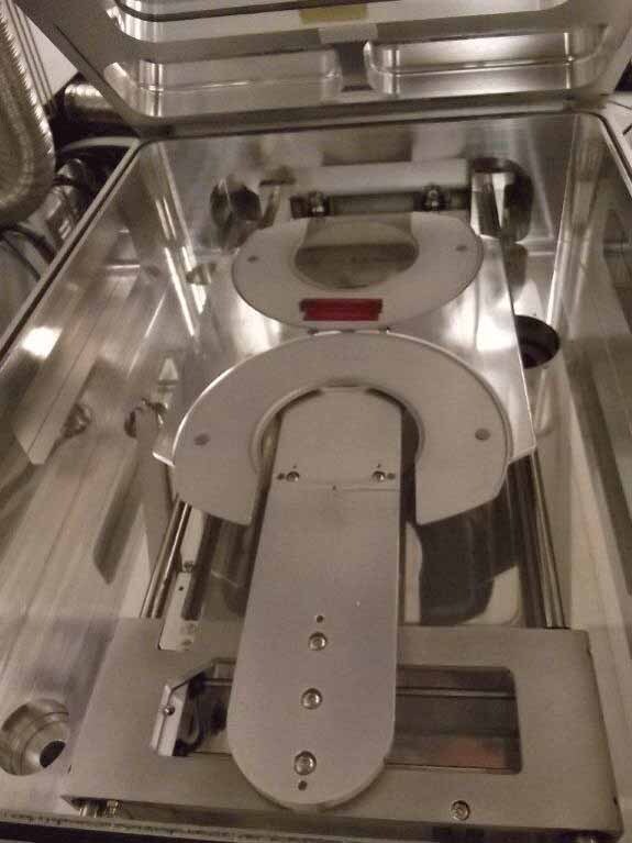
SR Etcher, 8"
Currently configured for 4"
Process: SiC, III-V, or Metal etch
Inductively coupled plasma source (ICP)
Carousel load lock (2-Wafer Carousel)
Heated lower chamber
Load lock chamber
Helium substrate backside cooling
Weighted clamp
ESR20N Vacuum pump (Chamber)
ALCATEL adixen ACP 40 vacuum pump (Load lock)
SMC Thermco chiller
E-Rack
MKS Spectrum 3KW 13.56MHz RF Generator (Source)
13.56MHz RF Generator (Lower electrode)
LEYBOLD MAG 1500CT Turbo pump
System cables (Full set)
SPTS System software
Gas configuration:
O2 - 50 SCCM
C4F8 - 200 SCCM
SF6 - 200
Ar - 200 SCCM
He - 200 SCCM
CF4 - 200 SCCM
CHF3 - 200 SCCM
NF3 - 200 SCCM
2007 vintage.
SPTS MPX ICP (Inductively Coupled Plasma Etcher/Asher) is a state-of-the-art etching tool used for the fabrication of ultraminiature structures in the sub-micron scale. It is one of the most versatile tools in the semiconductor industry, capable of both etching and ashing (thinning) wafers. MPX ICP uses inductively-coupled plasma technology to remove material from the surface of a wafer. A radio-frequency (RF) generator sends out an alternating current to an antenna coil, generating an electric field. This electric field then induces an electric current in the plasma—a gas containing positively and negatively charged particles—causing it to heat up and become ionized, emitting light and extreme temperatures in the range of 10,000°C. The high-temperature gas-ionized plasma is used to achieve accurate and repeatable etching control as the process is very selective when it comes to etch rates and profiles. Several plasma recipes are available for etching different materials and structures, including Si, SiO2, GaAs, and Cr. The etch rates of plasma processes usually range from 0.1-1000 nanometers per minute; enabling the etching of intricate features in the sub-micron range. SPTS MPX ICP also features a number of process control capabilities and can process a range of substrate sizes from 2 - 8" in diameter. It also offers a variety of process parameters to manipulate such as RF power, ICP pressure, gas flow, and etching time. The system is able to provide both constant and alternating etching procedures and has an optional wafer temperature controller, which is used to ensure accurate etching profiles and minimize the microwavable effect. In addition, MPX ICP offers many advantages such as low damage to the wafer surface, high-precision ashing, uniform etching, clean-surface-topography, high yield, and minimal contamination of the chamber. The system's remote monitoring capability and fast recipe development also boost its performance and make it a reliable option for most etching and ashing needs. Overall, SPTS MPX ICP is a very useful tool for etching and ashing operations in the semiconductor industry. It is a perfect choice for microfabrication of the most intricate structures, and its versatility and range of process parameters offers wide-ranging precision capabilities.
There are no reviews yet


