Used TEL / TOKYO ELECTRON ALD #293820202 for sale
URL successfully copied!
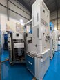
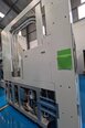
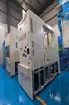
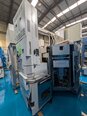
Tap to zoom
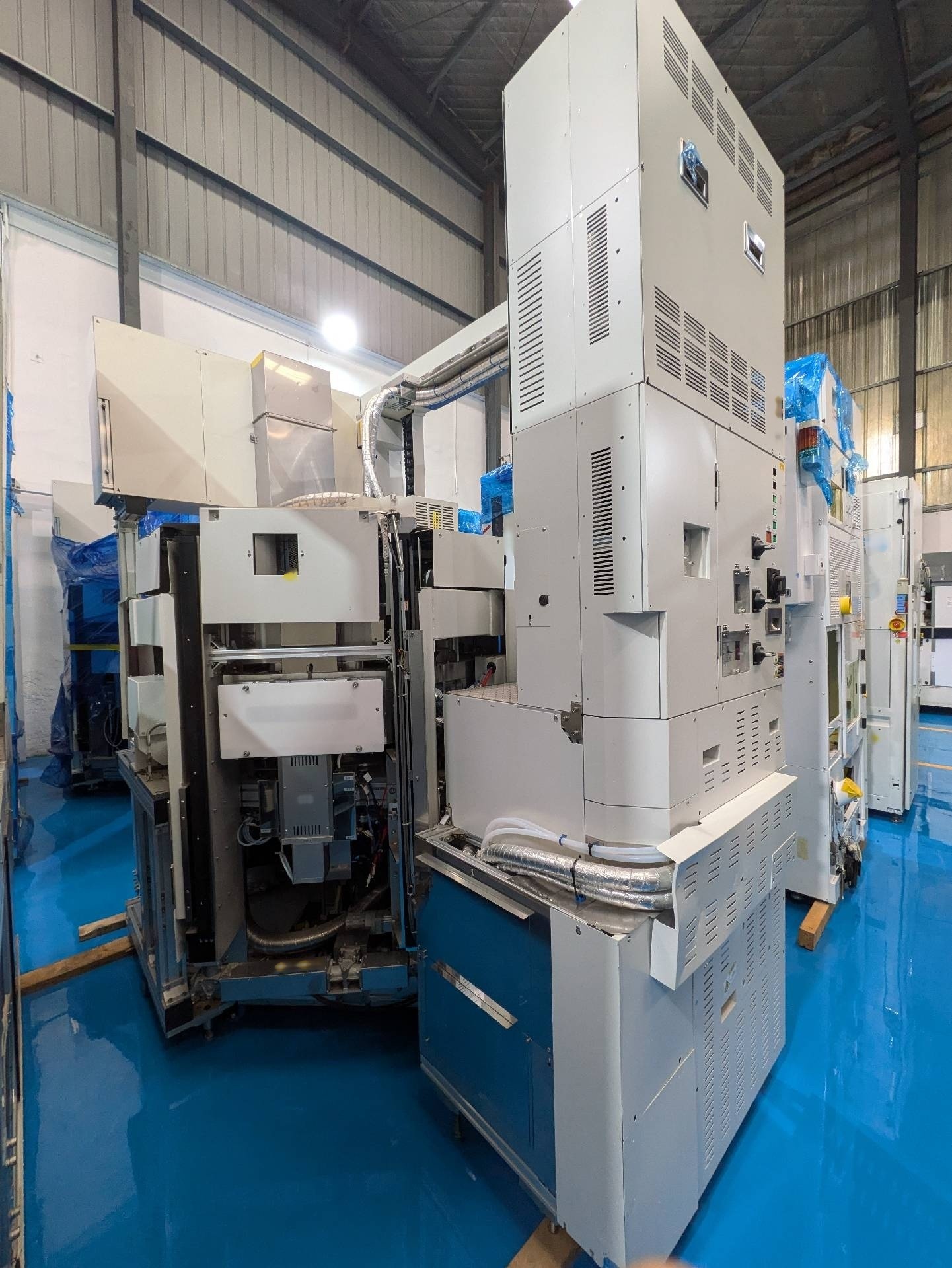

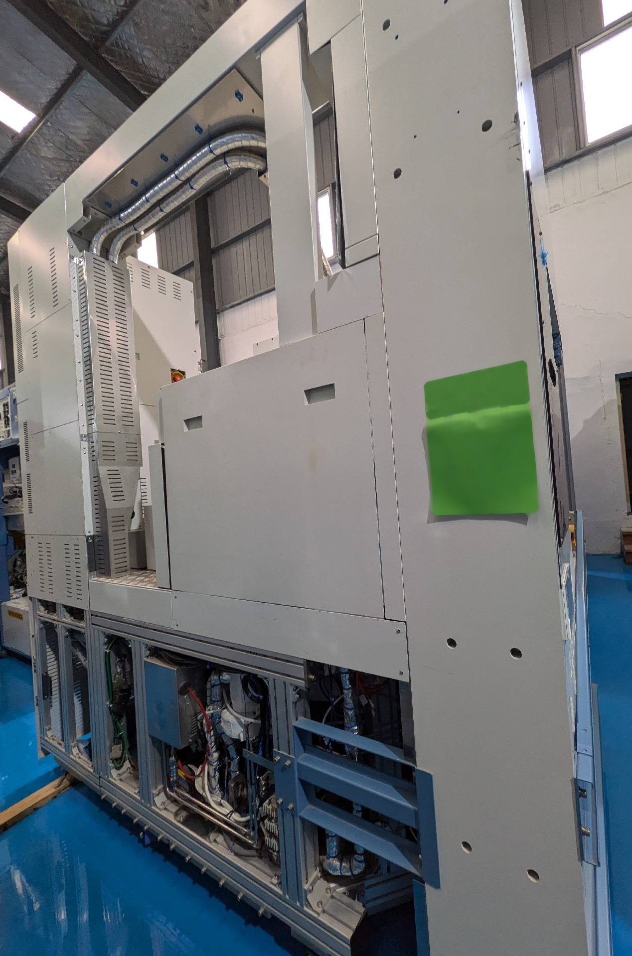
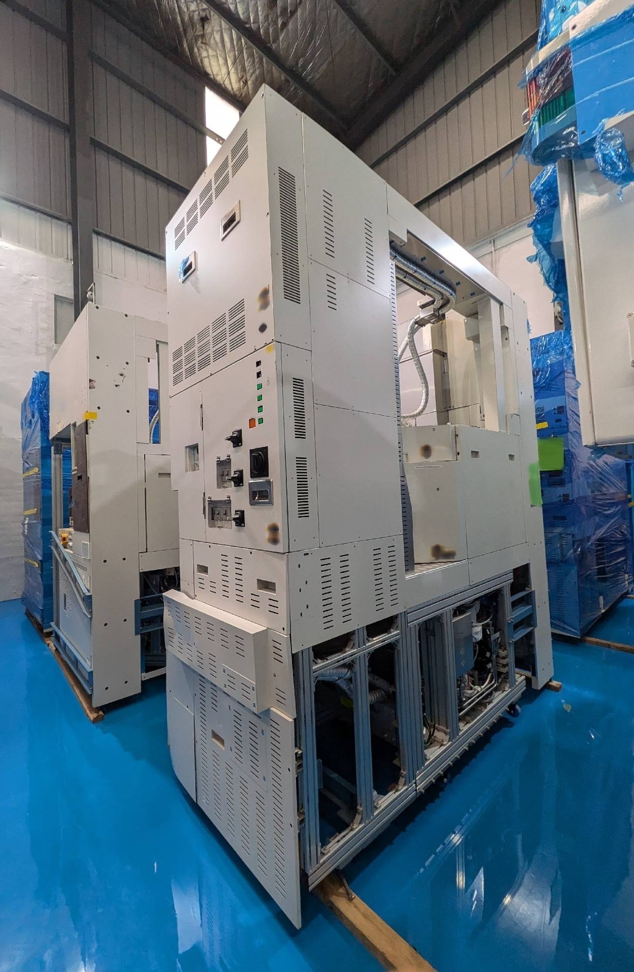
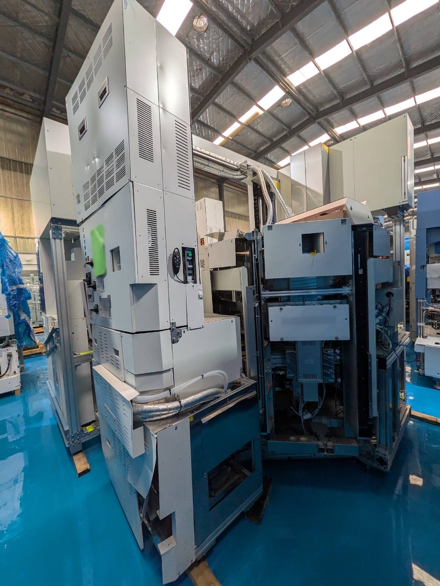
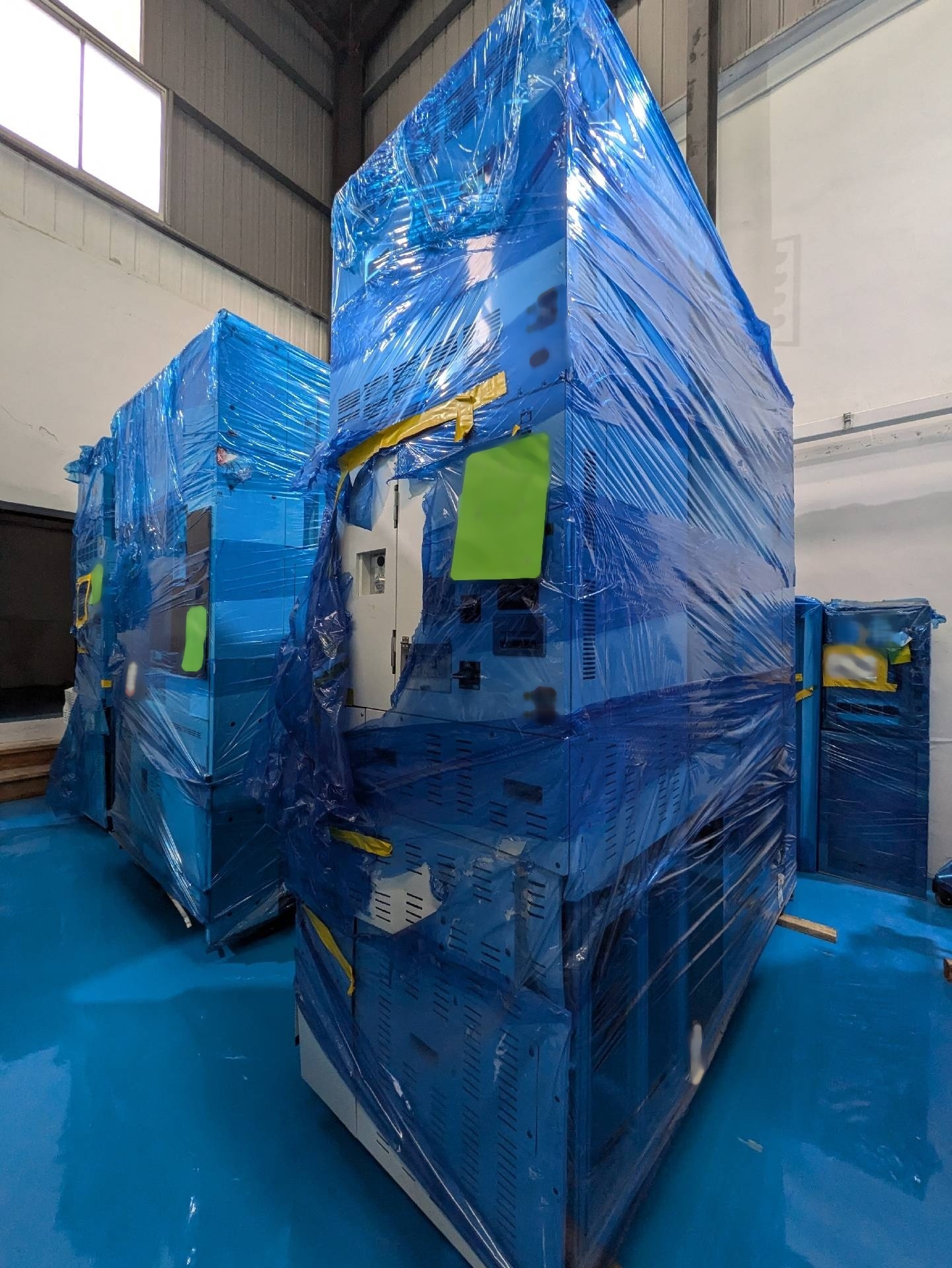
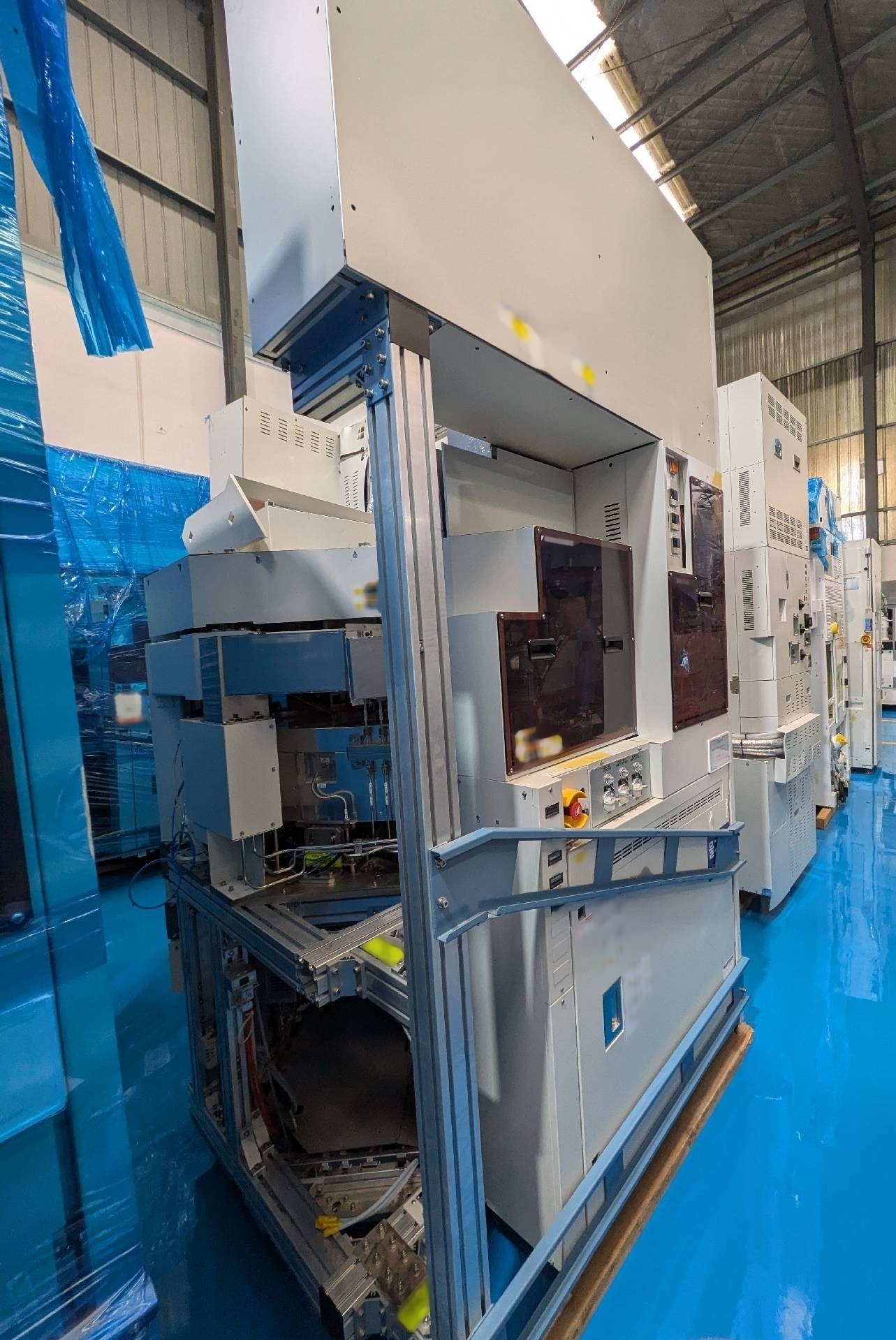
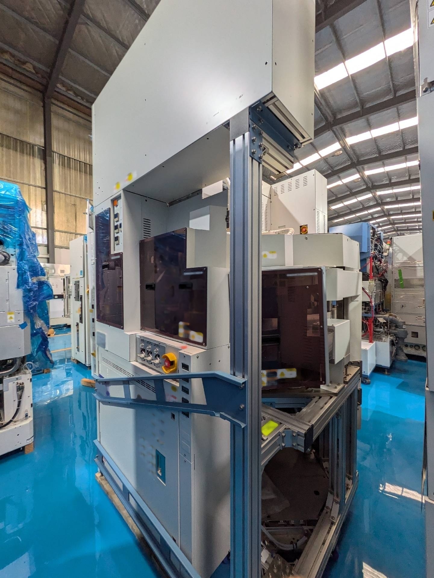
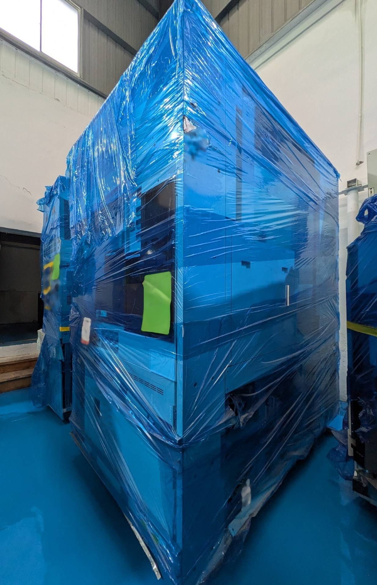
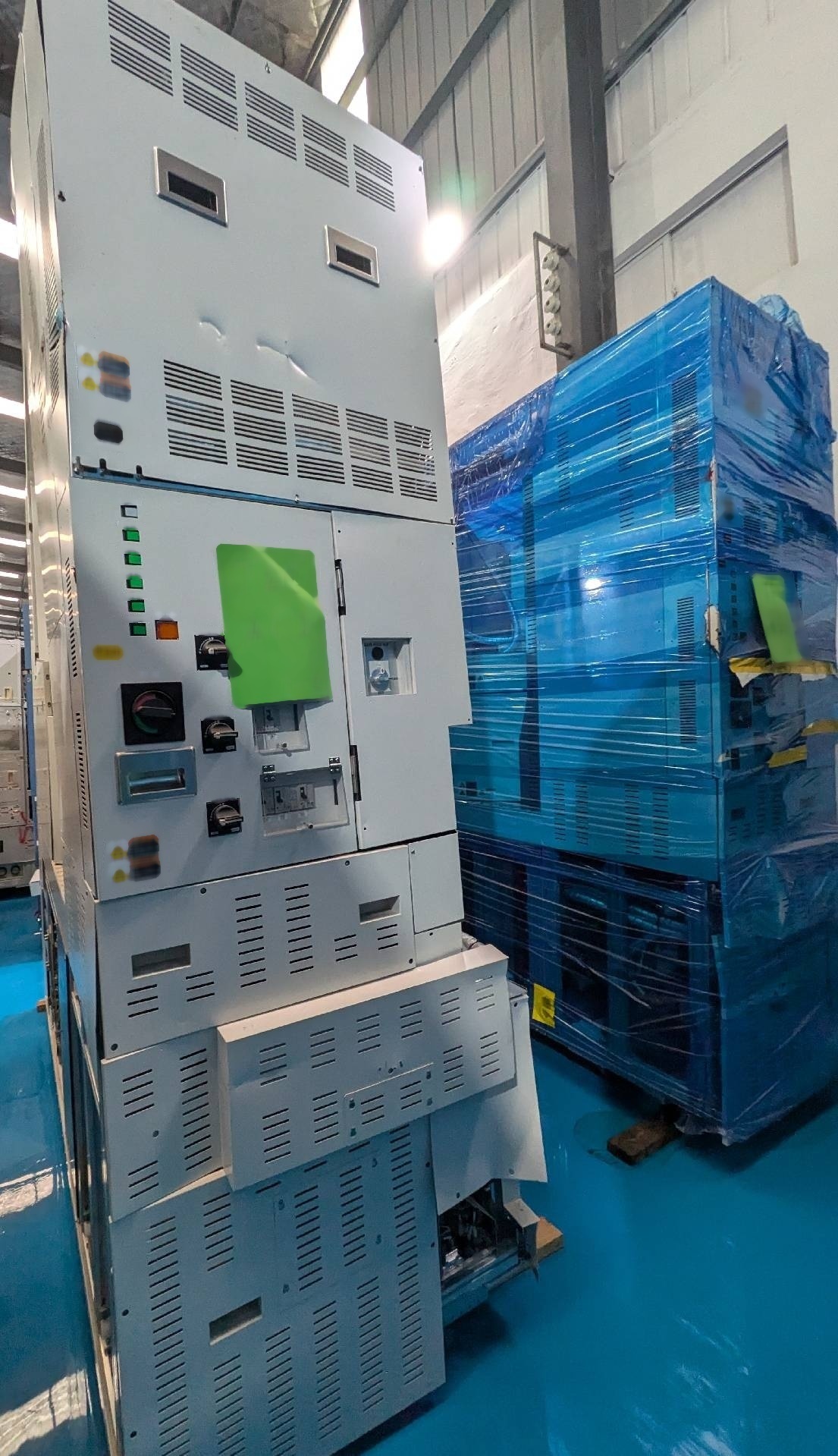
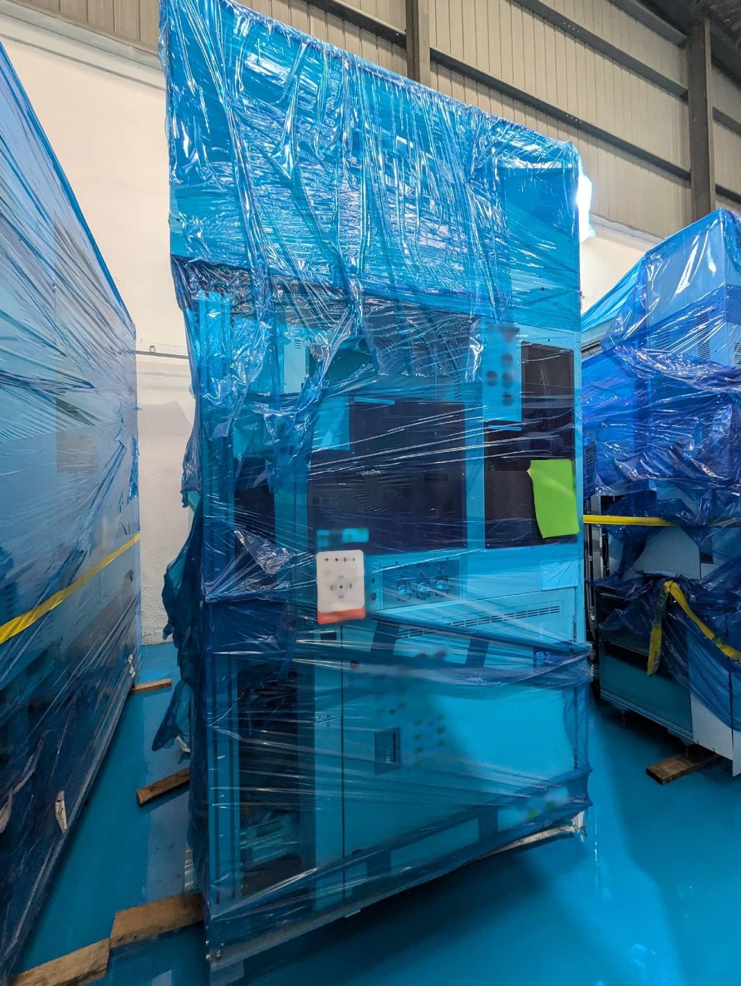
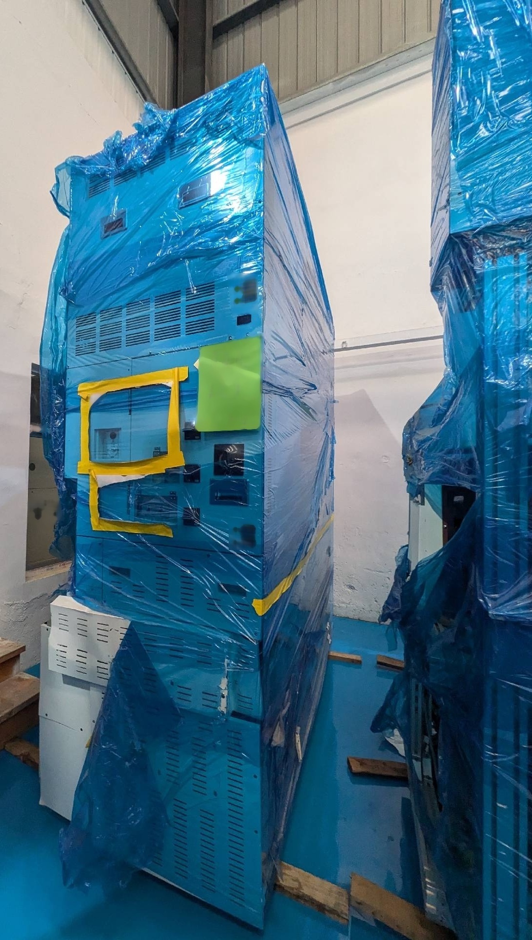
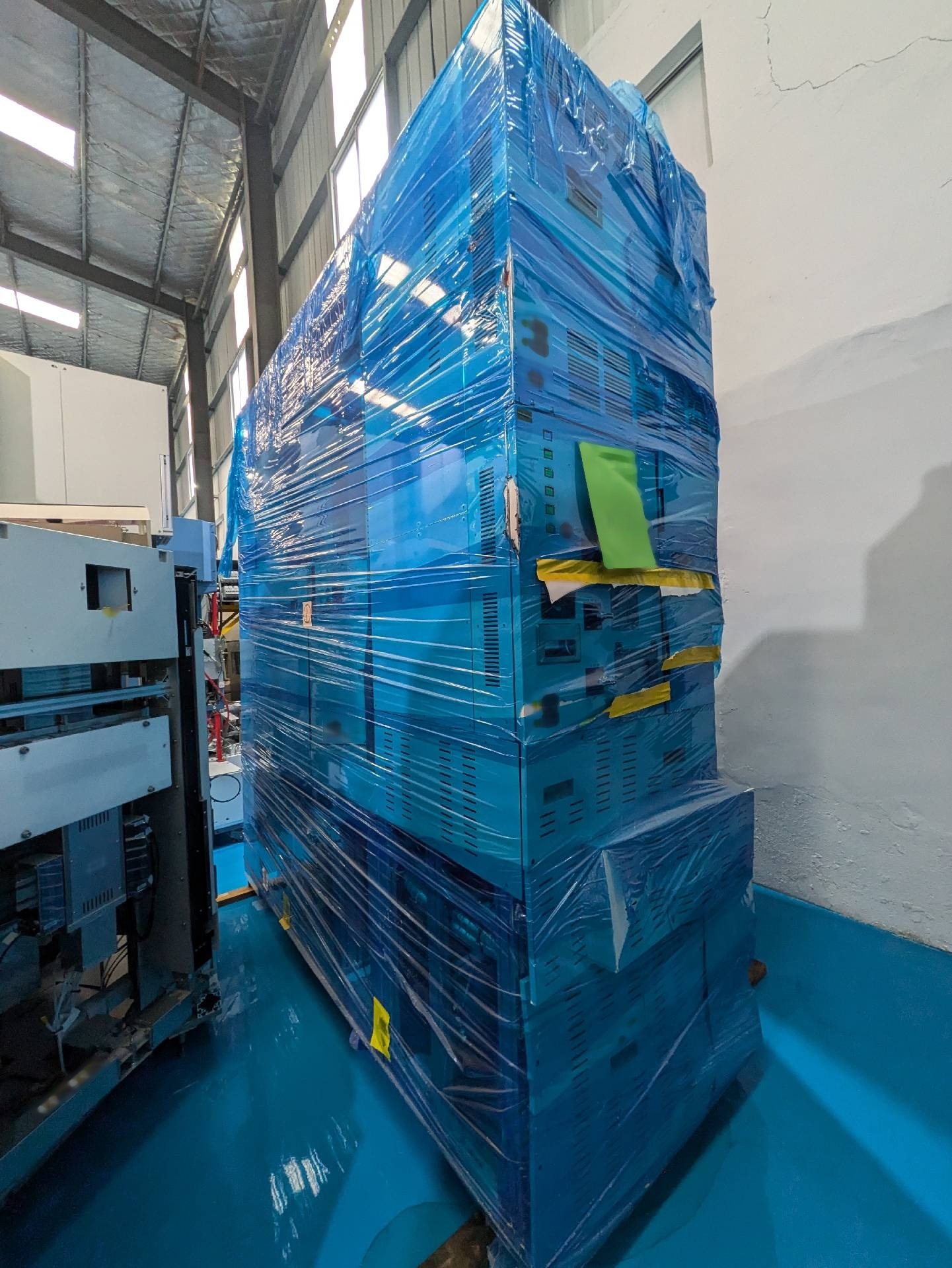
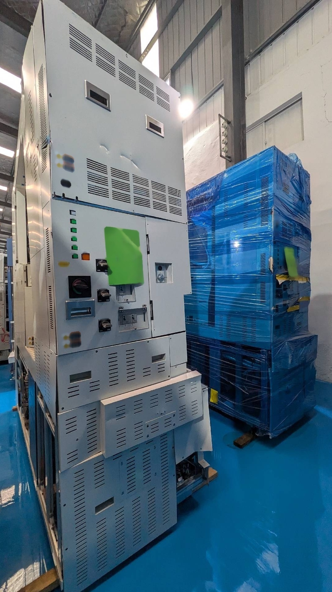
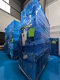
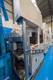
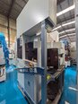
TEL / TOKYO ELECTRON ALD is a highly advanced etcher/asher equipment designed for semiconductor manufacturing processes. It combines the Atomic Layer Deposition (TEL ALD) technology with TEL expertise in plasma processing to provide a comprehensive solution for etching and ashing applications in the semiconductor industry. The system is equipped with a range of innovative features that enable precise and uniform etching/ashing of various materials used in semiconductor fabrication. TOKYO ELECTRON ALD technology is a key component of the unit, allowing for highly controlled and uniform deposition of thin films on substrates. This is achieved by sequentially exposing the substrate to precursor gases, which react with the substrate surface to form a thin film layer. The process is repeated multiple times to achieve the desired film thickness with atomic precision. One of the key advantages of ALD machine is its ability to coat complex 3D structures with high aspect ratios. This is particularly important in advanced semiconductor manufacturing, where the miniaturization of devices requires precise control over film deposition on intricate structures. The systemTEL / TOKYO ELECTRON ALD technology enables conformal coating of high aspect ratio features, ensuring uniform film thickness across the substrate. In addition to TEL ALD capabilities, the tool also integrates advanced plasma processing techniques for etching and ashing applications. Plasma etching is a key process in semiconductor manufacturing, used for patterning and structuring materials on the substrate. TOKYO ELECTRON ALD asset offers a range of plasma sources and process chambers optimized for different etching/ashing applications, providing flexibility to meet the diverse needs of semiconductor manufacturers. The model is equipped with advanced process control capabilities, including real-time monitoring of key parameters such as temperature, pressure, and gas flow rate. This allows for precise control over the etching/ashing process, ensuring consistent and reproducible results across multiple production runs. The equipment also features automated process recipes and recipe management tools, enabling easy setup and optimization of etching/ashing processes for specific materials and structures. Another key feature of ALD system is its advanced wafer handling capabilities. The unit can accommodate wafers of varying sizes and thicknesses, allowing for maximum flexibility in semiconductor manufacturing. The wafer handling machine is designed for high throughput production, with fast wafer loading and unloading times to minimize downtime and increase overall productivity. Overall, TEL / TOKYO ELECTRON ALD tool represents a state-of-the-art solution for etching and ashing applications in semiconductor manufacturing. By combining TEL ALD technology with plasma processing capabilities, the asset offers precise and uniform film deposition on complex 3D structures, enabling semiconductor manufacturers to achieve high-quality results with improved process control and productivity.
There are no reviews yet