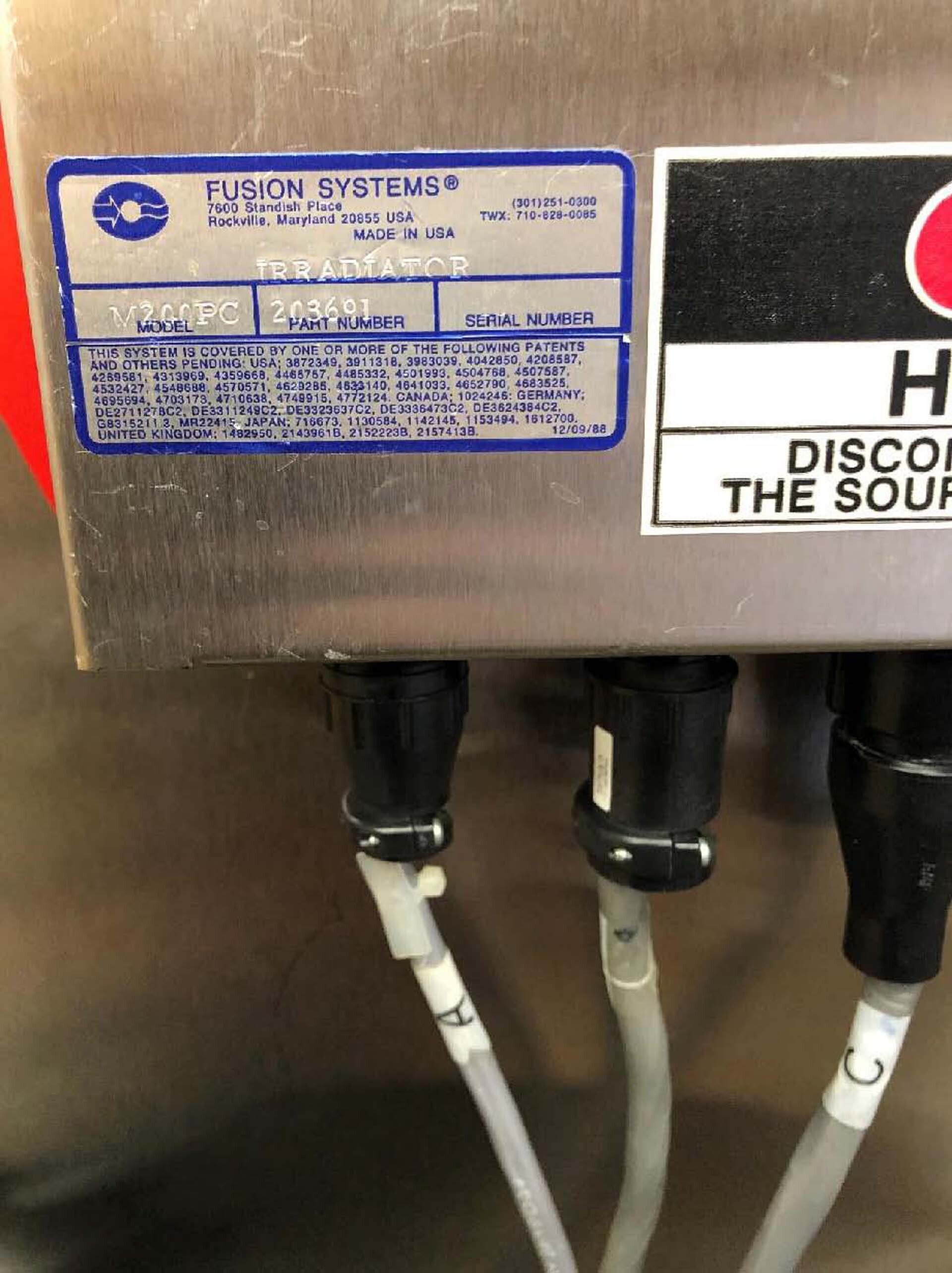
Used AXCELIS / FUSION M 200 PC #9266271 for sale
URL successfully copied!
Tap to zoom





























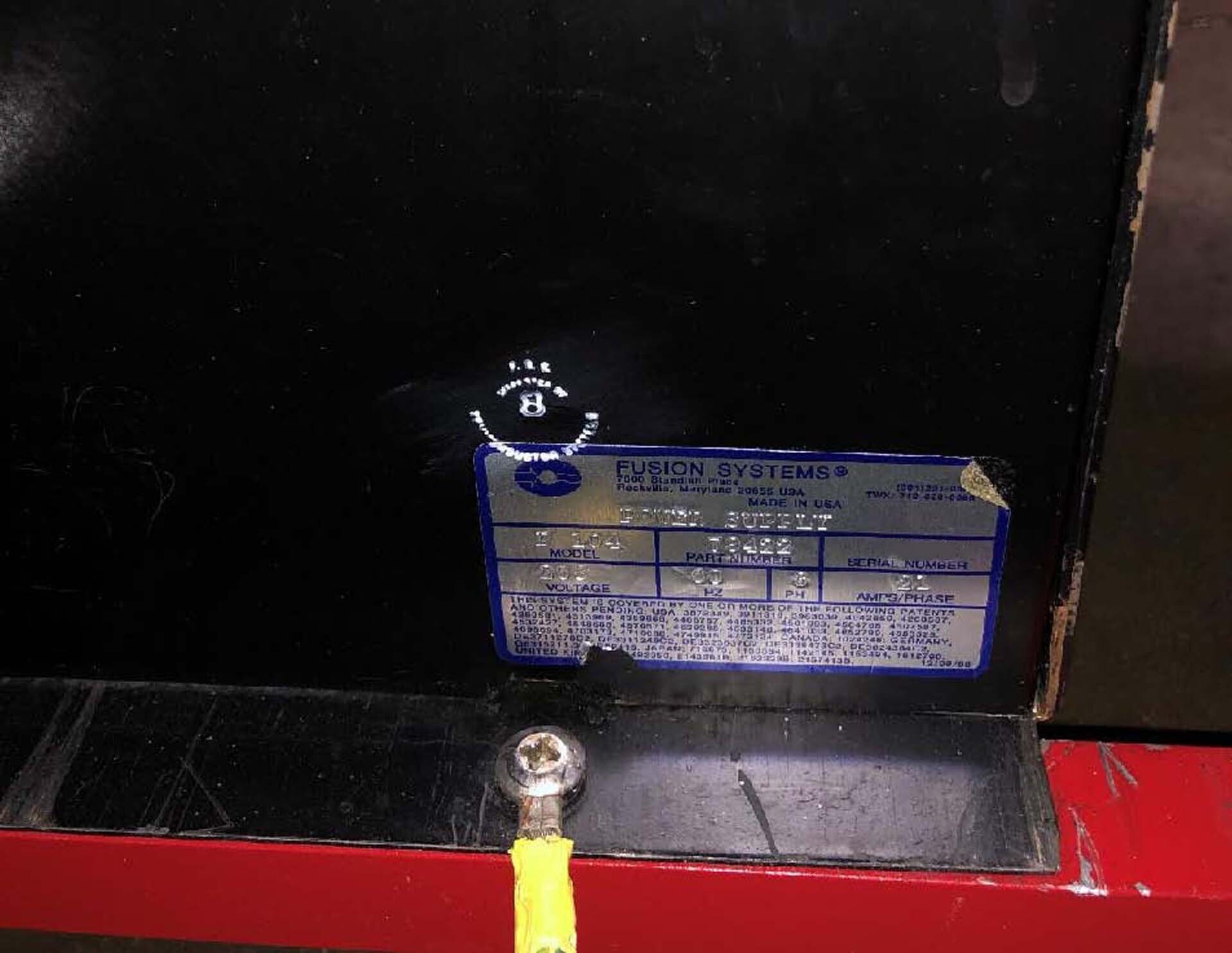

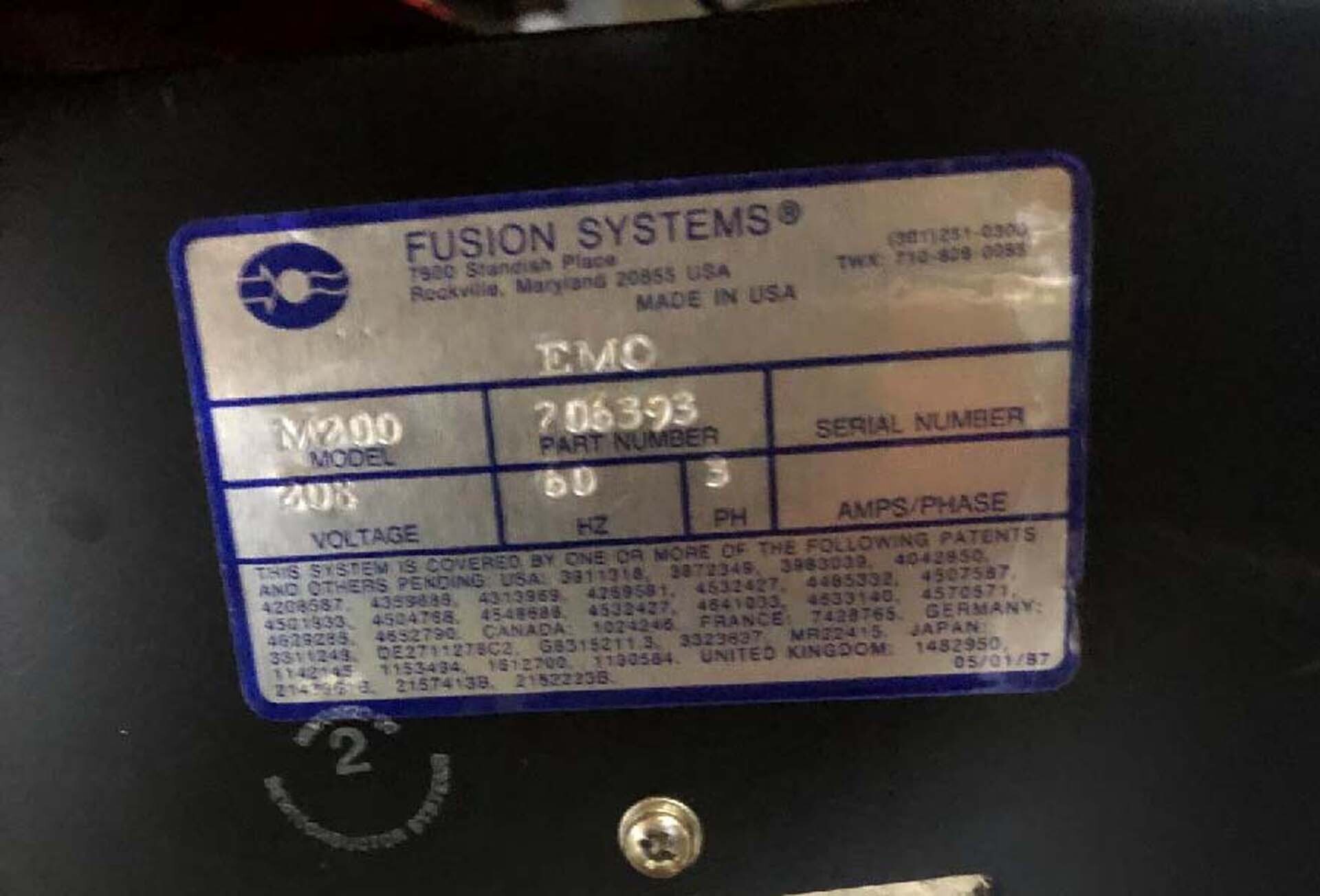

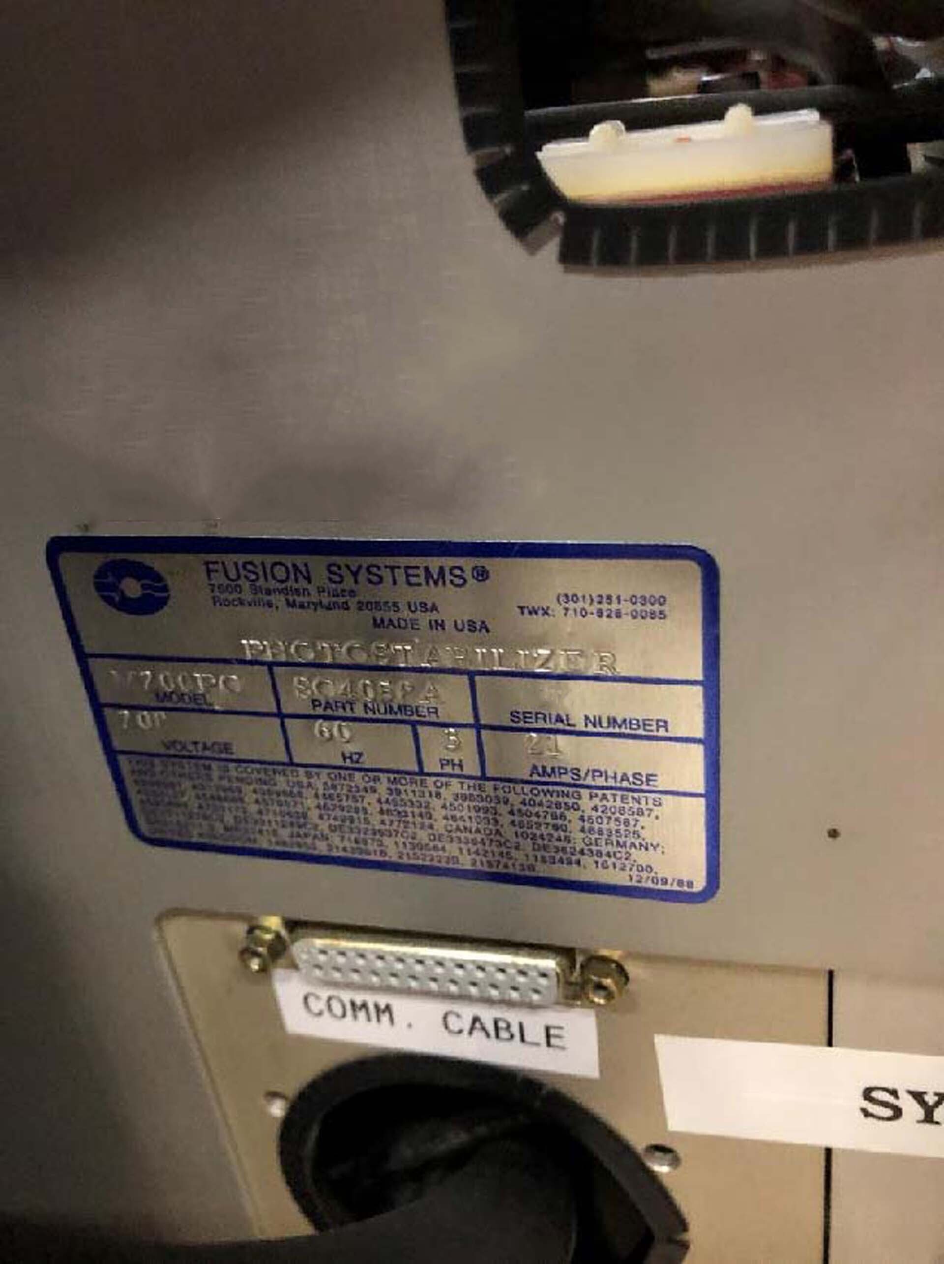

ID: 9266271
Vintage: 2006
Photo stabilizer
Wafer substrates, 3"-6"
Cassette to cassette hander
UV Light exposure with photoresist / Substrate temperature
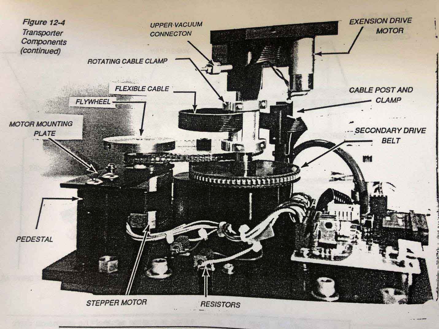
Transporters: Robotic pick and place
Lamp functions: Off, flash, low and high
Chuck temperature range: 50-240 iaC
Chuck temperature ramp rate: 0.5-2.5 iaC/sec
2006 vintage.
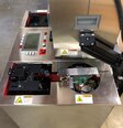
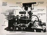
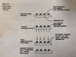
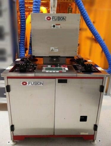
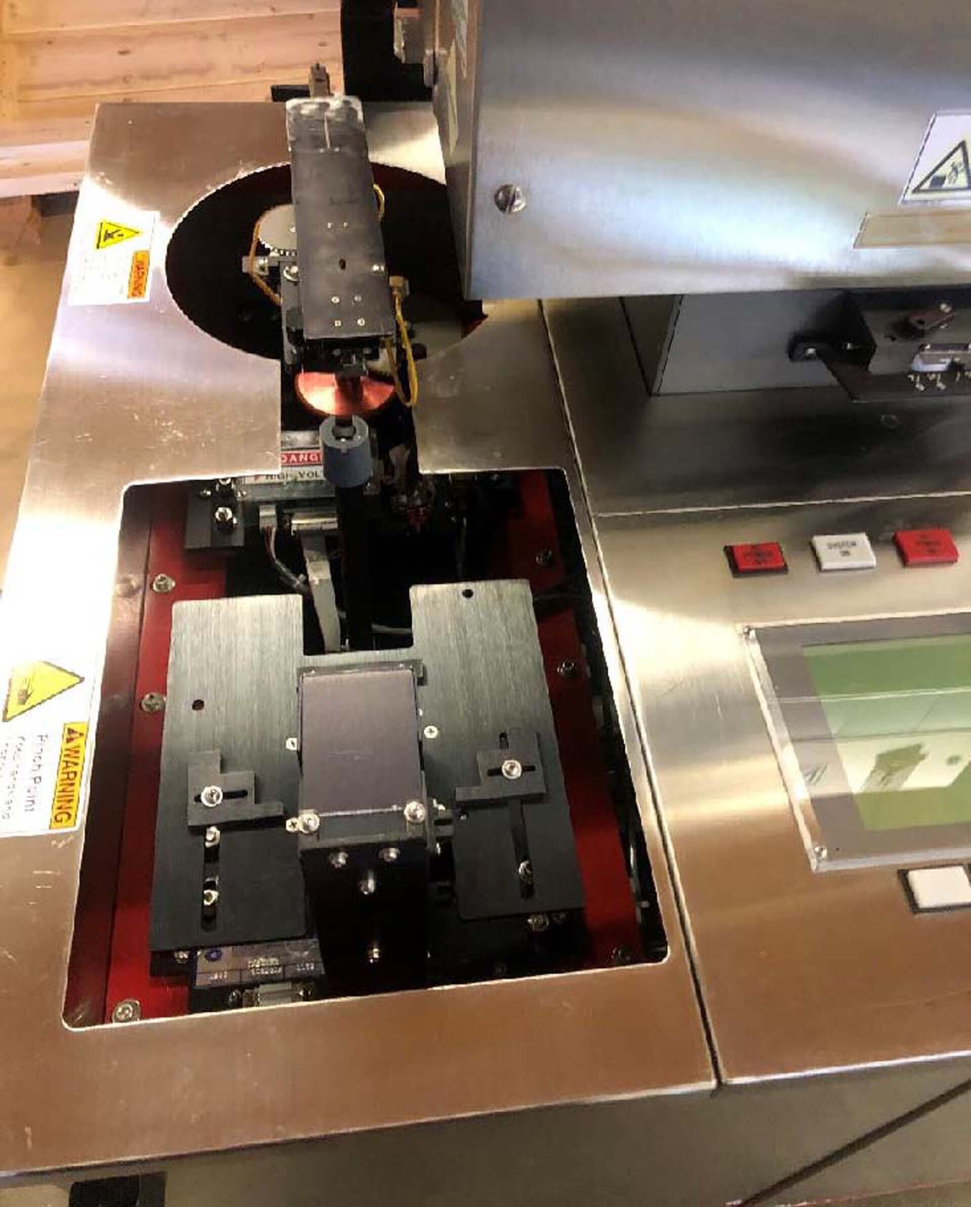
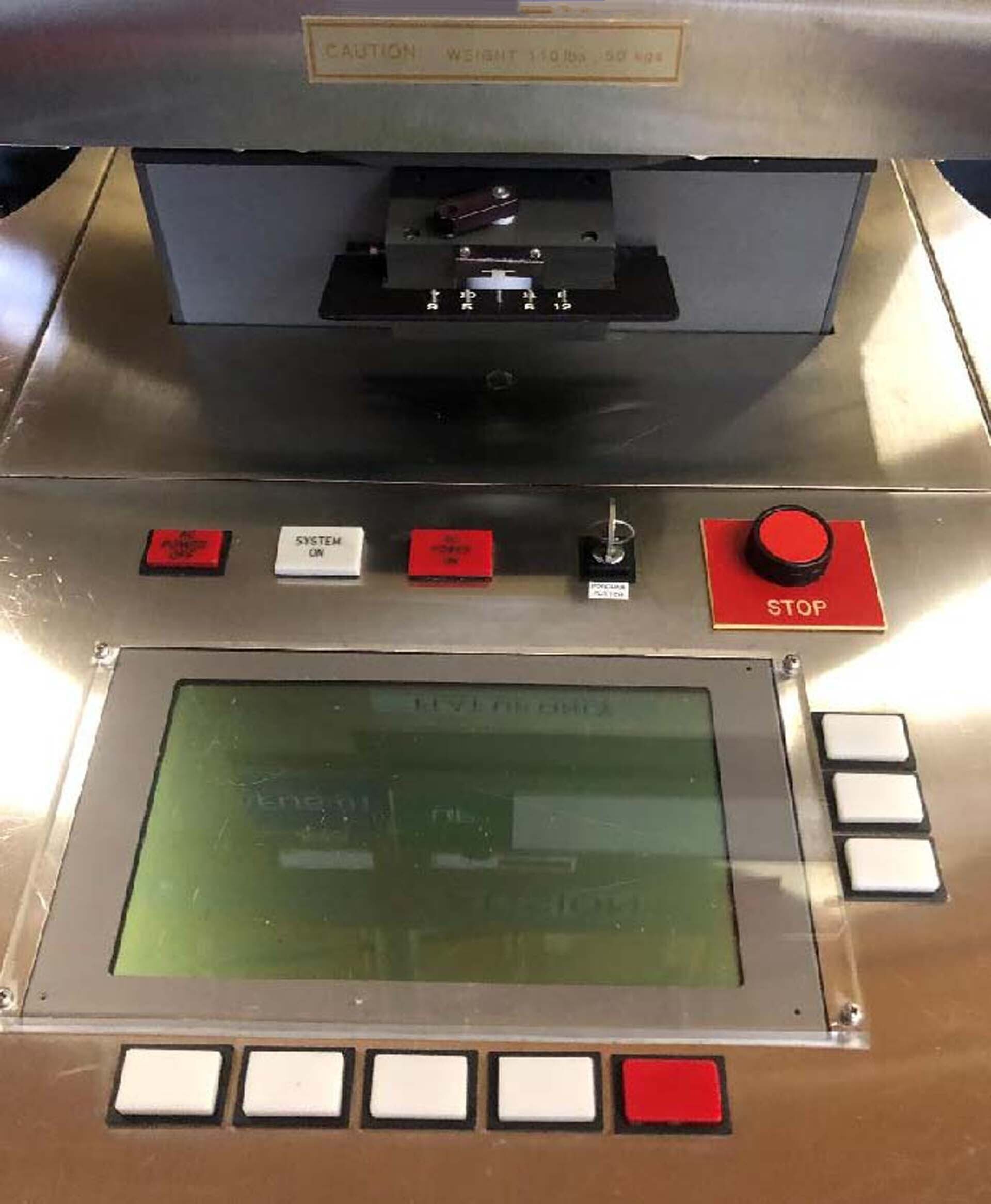
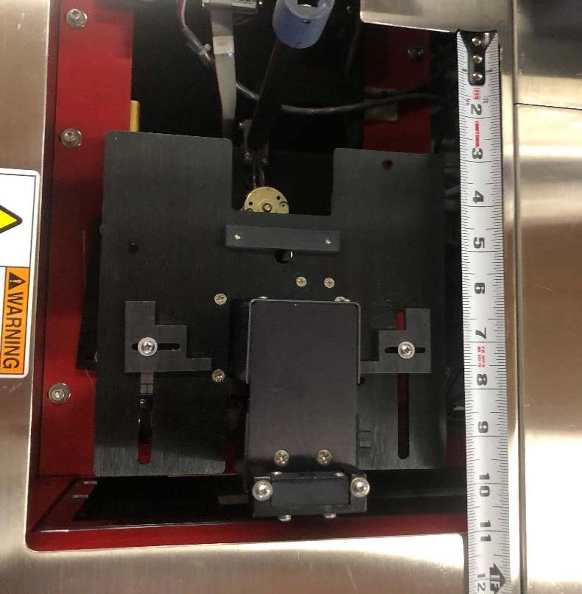
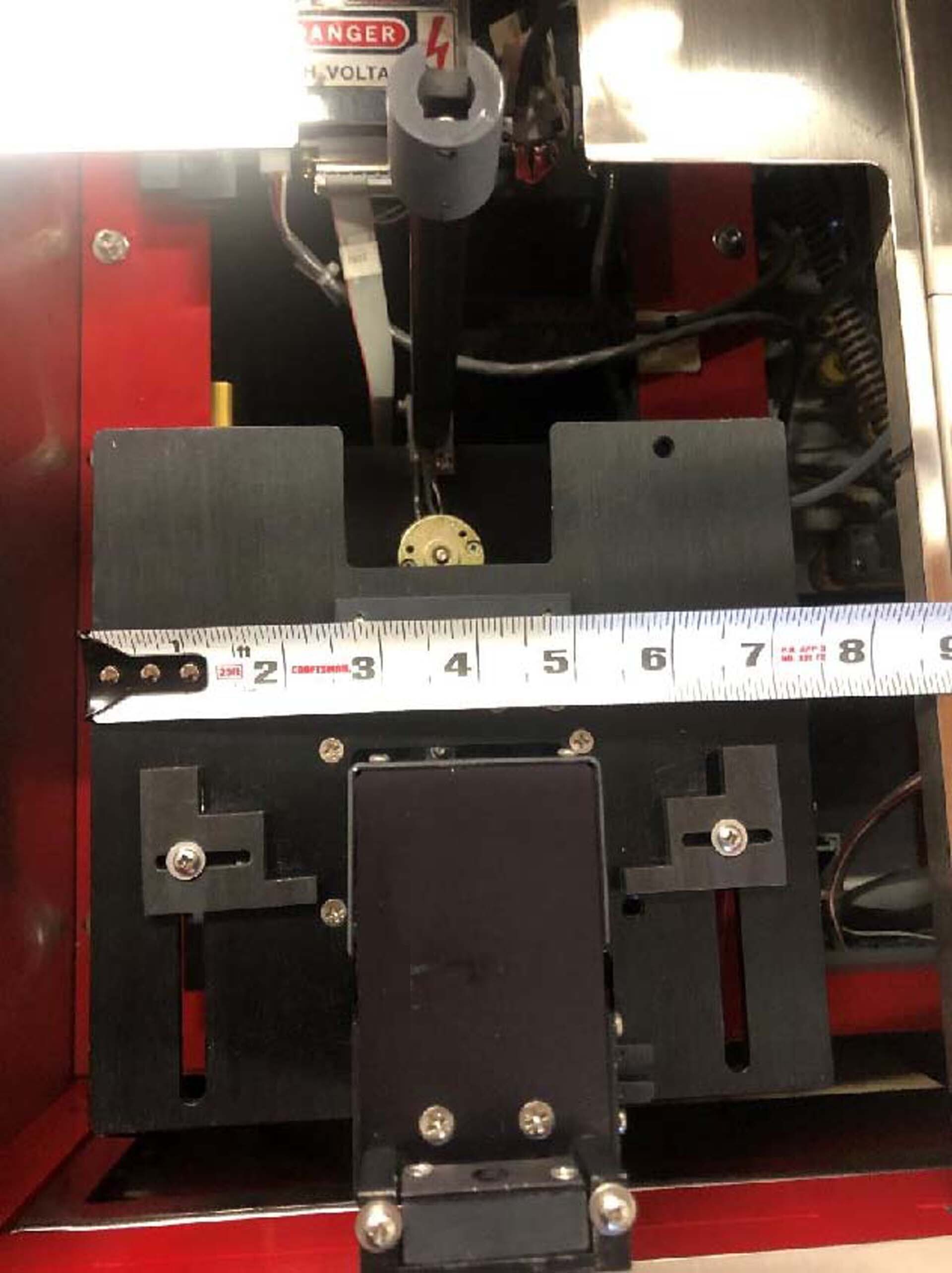
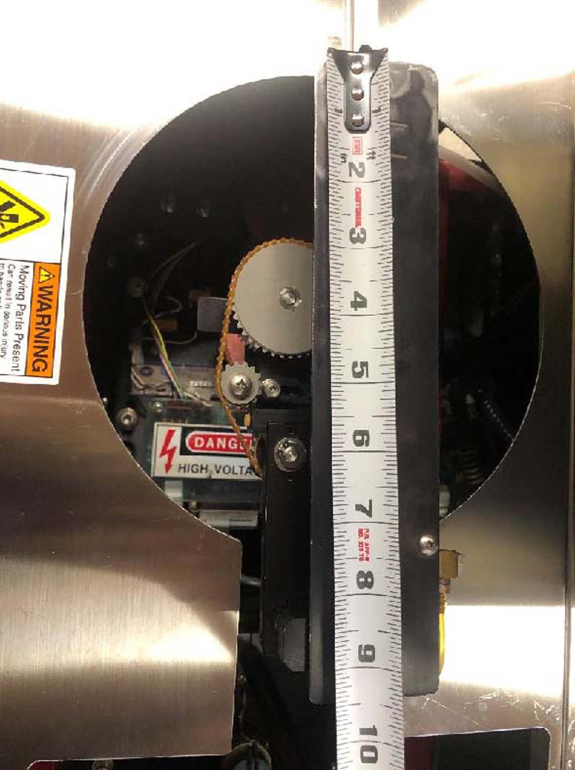
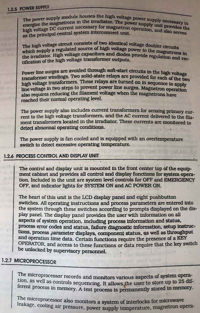
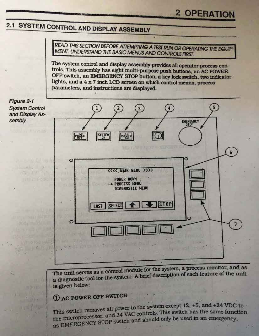
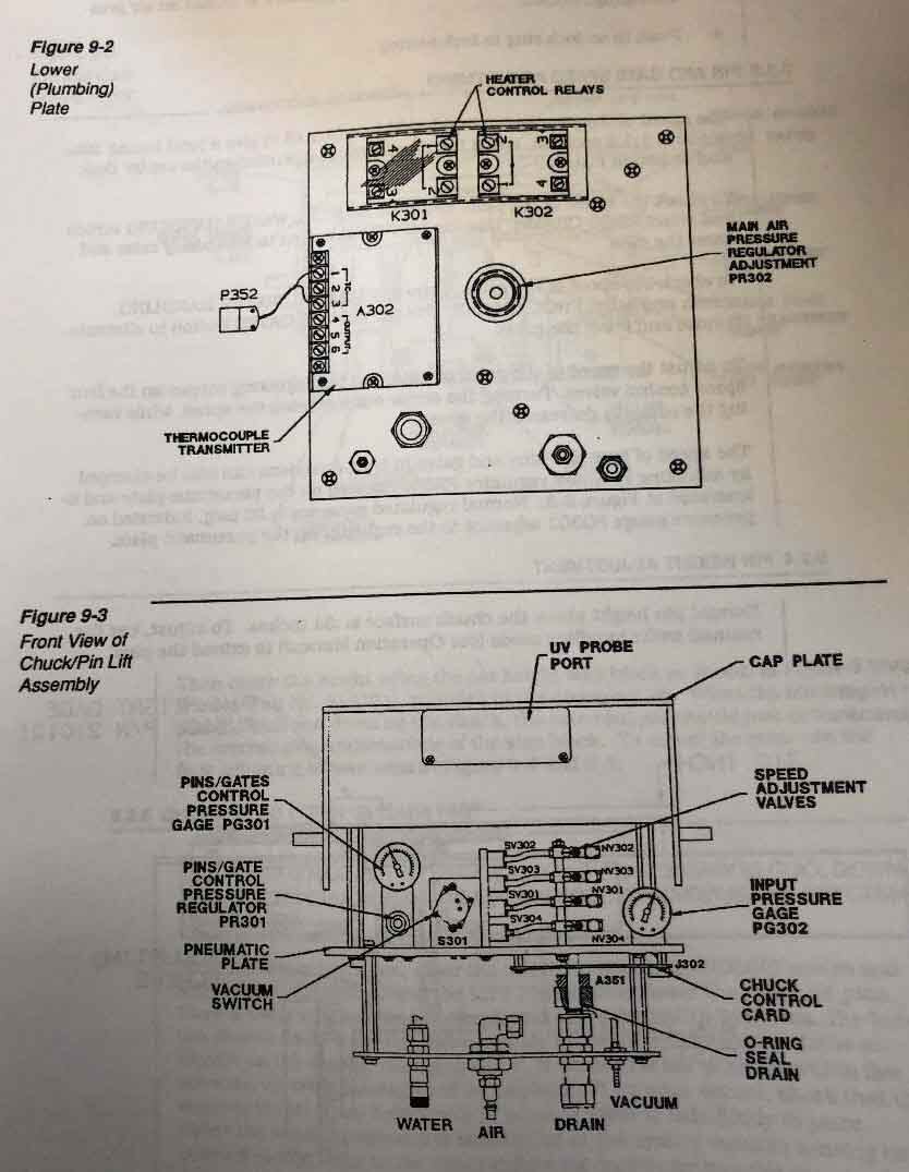
AXCELIS / FUSION M 200 PC is a state-of-the-art, high-precision wafer exposure equipment designed for product development, prototyping and production lines. The system features a variable-aperture, high-precision exposure microscope with a maximum resolution of 20μm/1μm across a field of view of 95 x 95 mm. The unit is engineered for applications such as lithography, advanced packaging, MEMS, thin-film photovoltaics, and biomems. The machine's large mechanical subsystems provide in-line automatic wafer alignment, wafer-focusing and format-conversion functions. The automated wafer alignment, coupled with a closed-loop focus-control and wide focus-range capabilities, provides accuracy and repeatability in the alignment of multiple wafers. An integrated wafer-handling tool accommodates all cassettes, wafer pods, flat and bowed substrates, wafers with large numbers of bumps, braid and eutectic bonding, and MEMS inside vacuum packaging. The asset also features a space-saving scanner design, allowing for the integration of a 400mm wafer for process development. The scanner optical subsystem emphasizes performance over cost in order to achieve the highest resolution and precision available in off-the-shelf equipment. The optics, comprised of a high power short pulse laser diode, environmentally sealed lens assembly and field reduction optics, provide a light intensity of up to 200 mW/cm2 with a narrow spectral bandwidth. FUSION M200PC is designed to meet semiconductor industry demands for high yield, low-cost and defect-free waffles. A vision in-model calibration feature and an advanced wafer spacer control equipment increase cycle time and yields due to improved process flexibility and wafer tracking. In addition, flexible application-supported operation ensures continuous feedback on recoverable errors, and automatic laser cleaning eliminates particle contamination and increases yields. The system also includes intuitive, user-centric software enabling control of the entire unit, including pre-deposition light exposure. With an intuitive drag-and-drop user interface, users can design their lithography jobs, control parameters and monitor the process in real time. The software also includes an exposure log with an in-machine database for storing and displaying past job runs. Overall, AXCELIS M200 PC delivers precise and repeatable performance and unmatched repeatability across a variety of wafer formats, making it an ideal choice for semiconductor fabrication. It is the perfect tool for process development and production, where fast changeovers and on-board data logging produce high yields and excellent results.
There are no reviews yet


