Used HAKUTO HAP-1100ST #293793158 for sale
URL successfully copied!
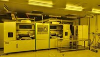
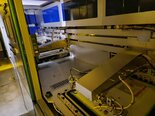



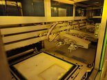
Tap to zoom
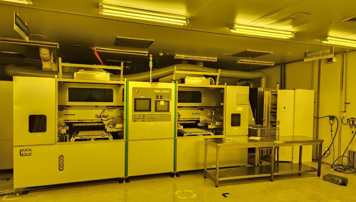

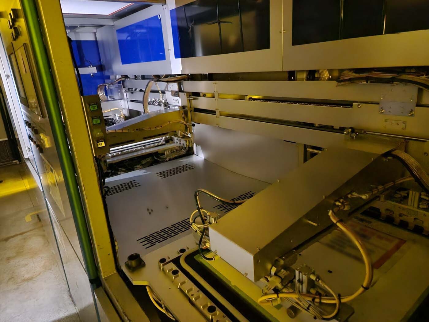
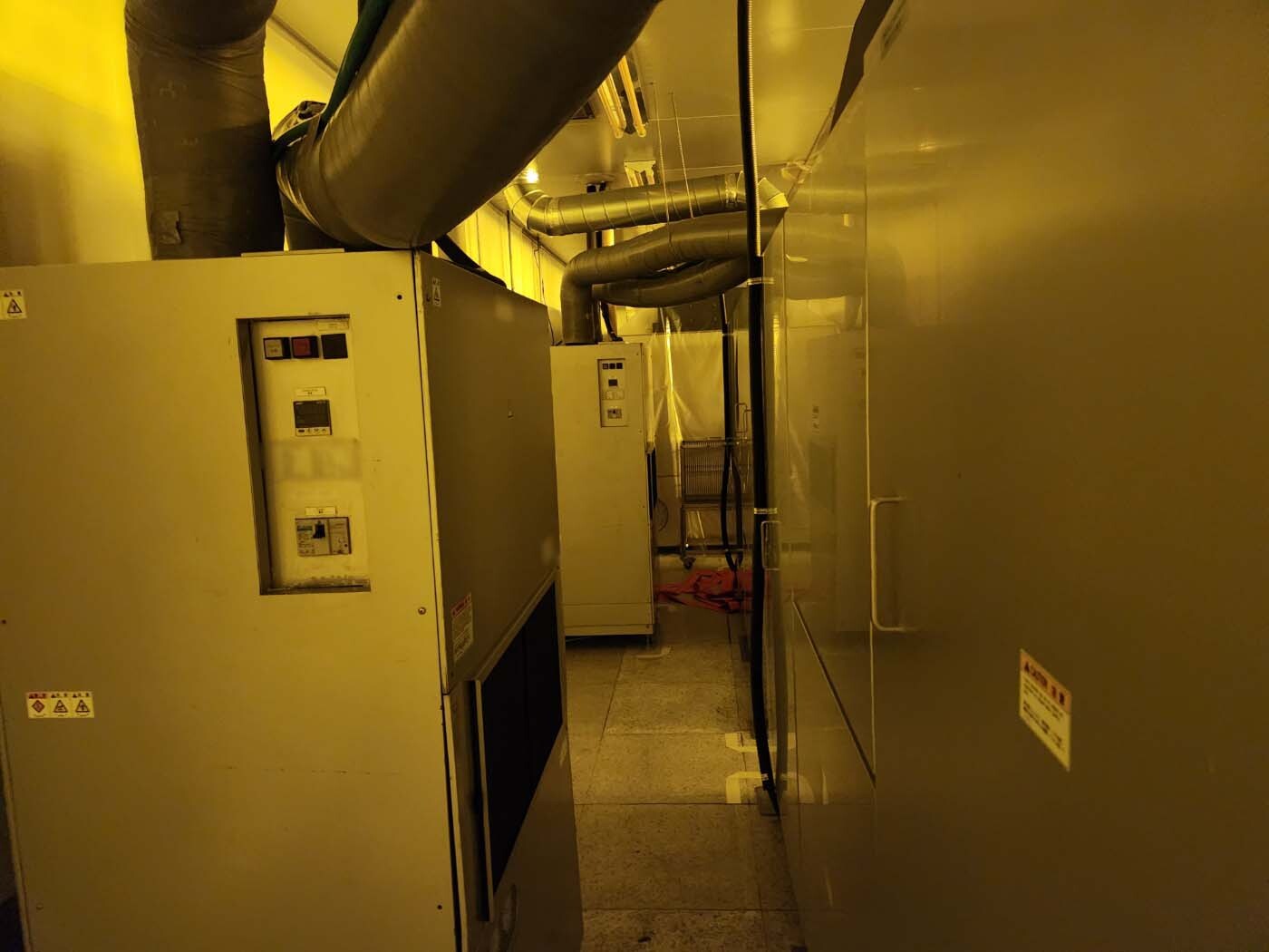
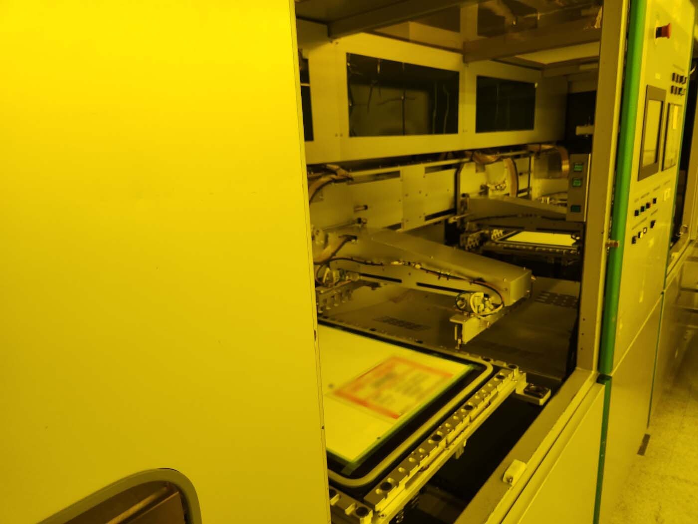
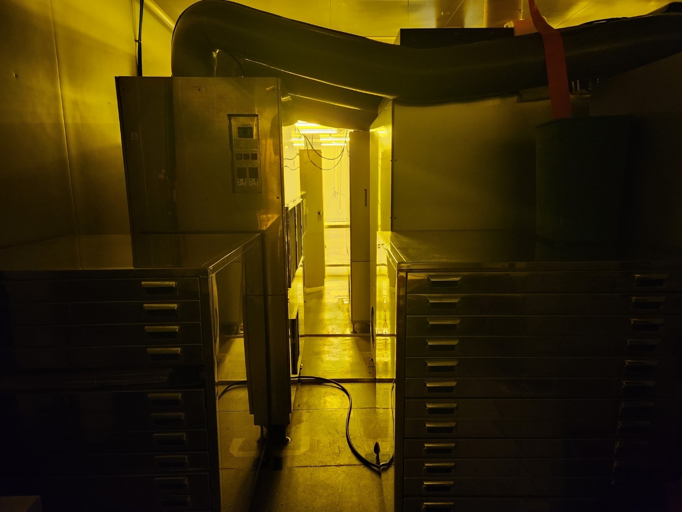
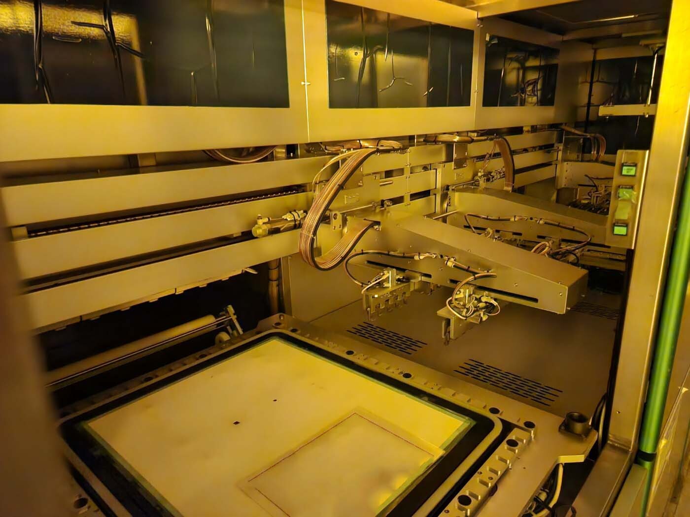
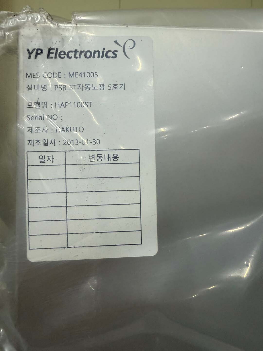
ID: 293793158
Vintage: 2013
Automatic exposure system
CCD Camera
IR lighting
Vacuum sealing
UV Lamp
Loading and unloading conveyor
Temperature controller
HEPA Unit
LCD Touch panel
Power supply: 220 V, 3 Phase, 50/60 Hz
2013 vintage.
HAKUTO HAP-1100ST is an advanced exposure equipment that is designed for high precision and reliable performance in the semiconductor manufacturing industry. This cutting-edge system incorporates a range of innovative features to meet the demanding requirements of mask and wafer lithography processes, enabling manufacturers to achieve unmatched levels of accuracy and productivity. At the core of HAP-1100ST exposure unit is its state-of-the-art projection optics, which play a crucial role in defining the pattern transfer accuracy during the lithography process. The machine utilizes a sophisticated lens tool with a high numerical aperture (NA) to achieve exceptional resolution and image quality. This advanced optics design enables the asset to project intricate patterns onto the wafer with sub-micron precision, ensuring that the final device features meet the stringent specifications of today's semiconductor devices. In addition to its high-performance optics, HAKUTO HAP-1100ST is equipped with a robust mechanical platform that provides stability and repeatability during the exposure process. The model features a rigid frame construction and precise motion control mechanisms that minimize vibration and positioning errors, allowing for accurate alignment and exposure of the wafer. This mechanical stability is essential for ensuring the uniformity and consistency of patterns across the entire wafer surface, which is critical for achieving high yield and device performance. Furthermore, HAP-1100ST exposure equipment integrates cutting-edge alignment and calibration technologies to optimize the registration of mask patterns with the wafer. The system employs advanced alignment algorithms and high-speed stage positioning systems to precisely align the mask and wafer during exposure, ensuring that the patterns are transferred with sub-micron accuracy. This level of alignment precision is essential for controlling critical dimensions and overlay requirements in semiconductor manufacturing, where even minor misalignments can lead to device failure. HAKUTO HAP-1100ST exposure unit also features a range of advanced software capabilities that enhance its flexibility and efficiency in semiconductor lithography applications. The machine is equipped with user-friendly interface software that allows operators to easily program exposure parameters, monitor process status, and analyze results in real-time. Additionally, the tool supports advanced automation features, such as recipe management and data logging, to streamline the production workflow and improve productivity. Moreover, HAP-1100ST exposure asset is designed to meet the evolving needs of the semiconductor industry by providing compatibility with a wide range of mask types, including binary masks, phase-shift masks, and other advanced mask technologies. The model's versatile design and compatibility with various mask formats enable manufacturers to address diverse lithography requirements and accommodate different device designs with ease. Overall, HAKUTO HAP-1100ST exposure equipment represents a leading-edge solution for semiconductor manufacturers seeking to achieve superior patterning performance and production efficiency in their lithography processes. With its advanced optics, mechanical stability, precision alignment capabilities, and user-friendly software features, HAP-1100ST system offers a comprehensive solution for achieving high-quality device fabrication and meeting the stringent demands of modern semiconductor applications.
There are no reviews yet