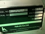
Used HAKUTO HAP-1510ST #293793160 for sale
URL successfully copied!


Tap to zoom

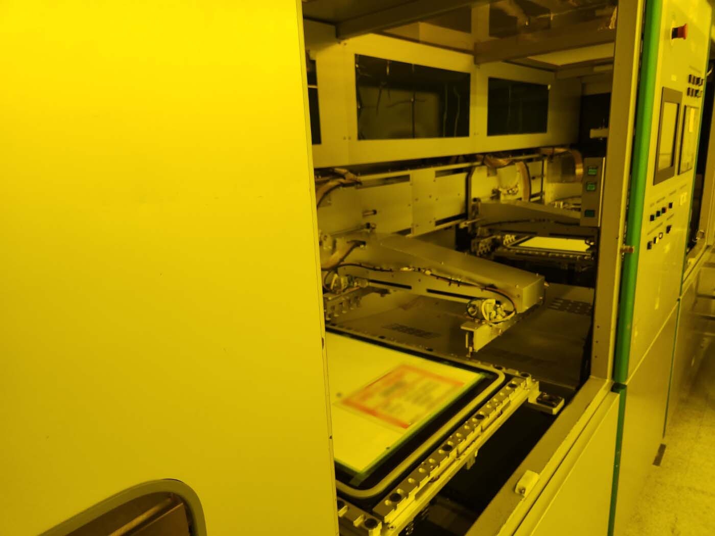
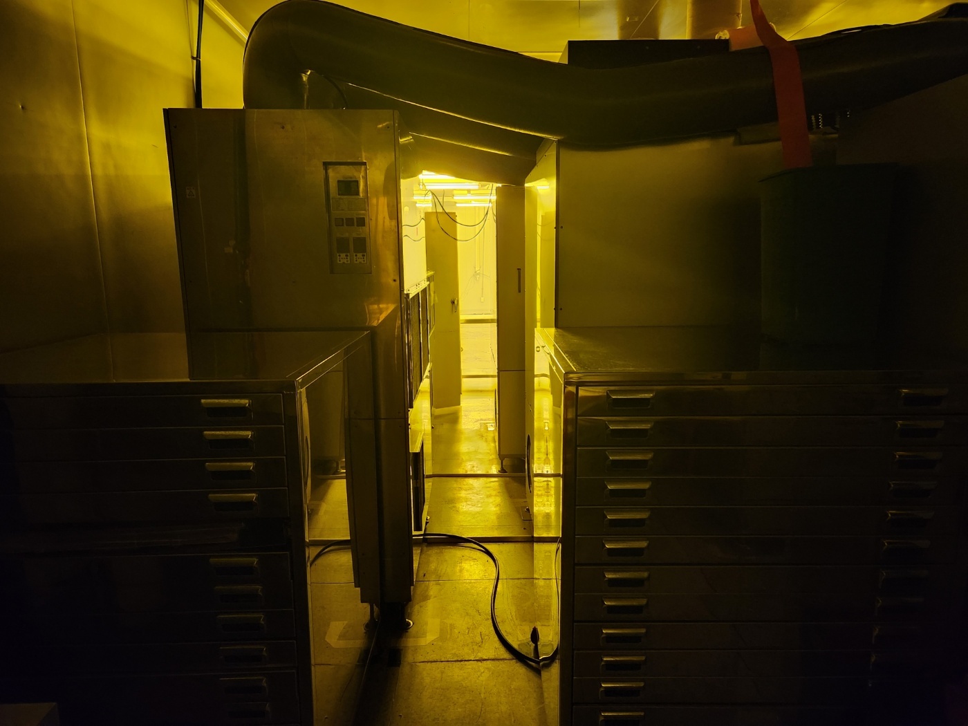
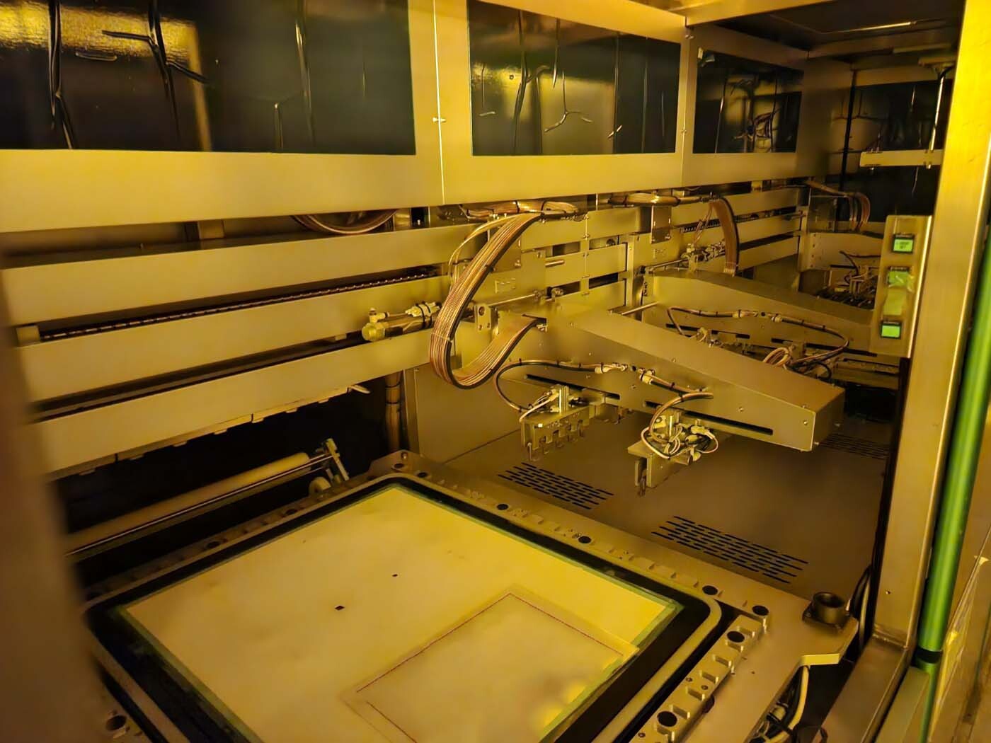
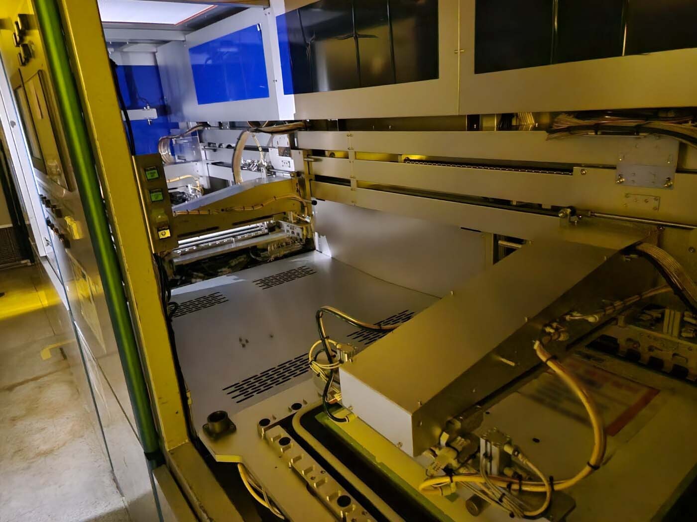
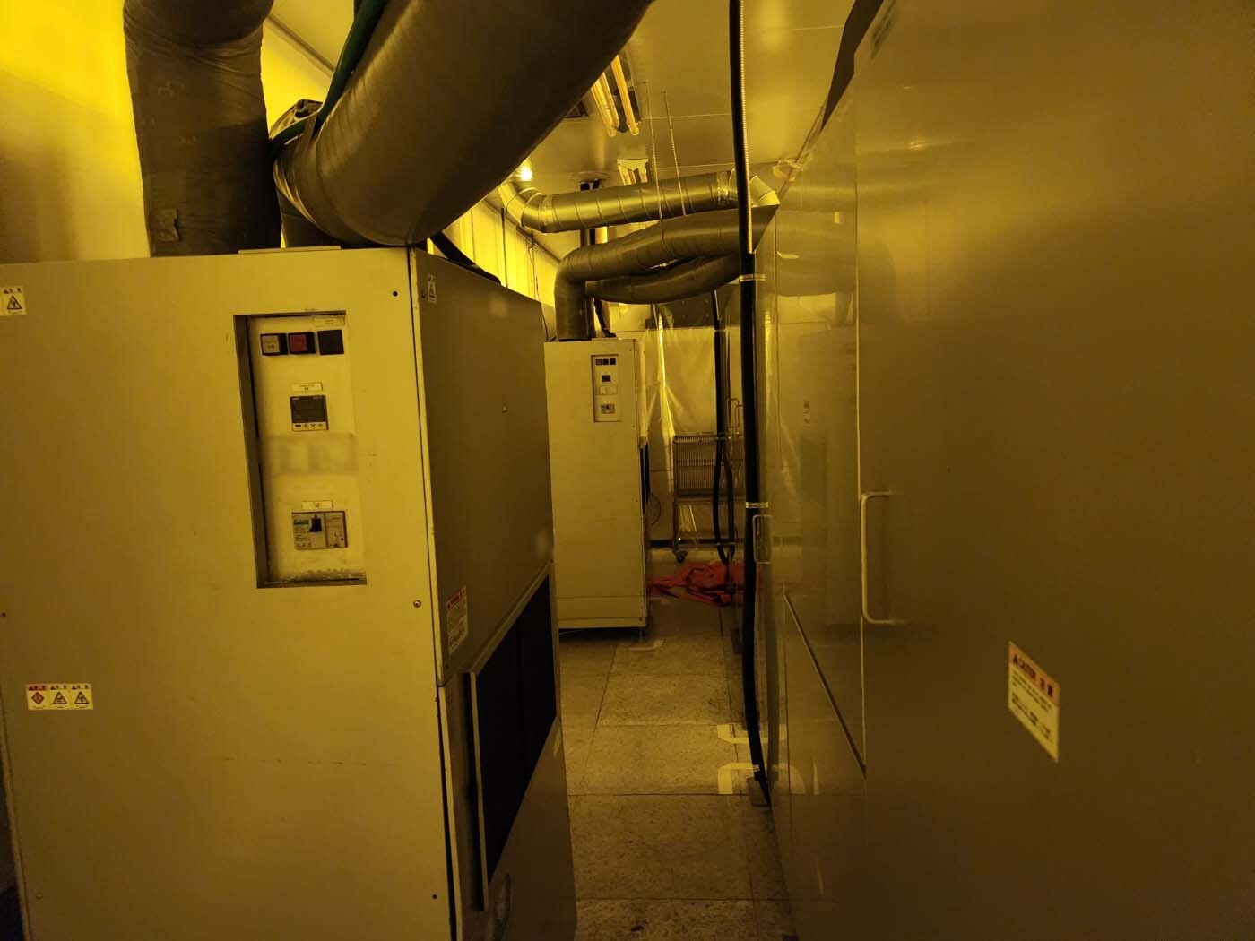
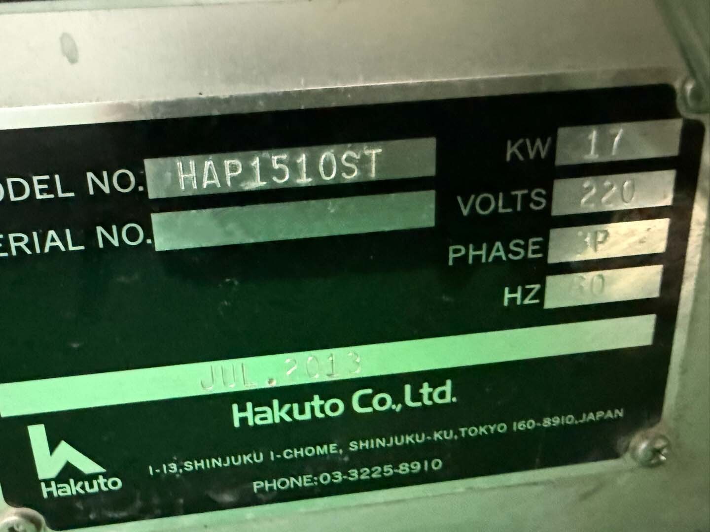
ID: 293793160
Vintage: 2013
Automatic exposure systems
CCD Camera
IR lighting
Vacuum sealing
UV Lamp
Loading and unloading conveyor
Temperature controller
HEPA Unit
LCD Touch panel
Power supply: 220 V, 3 Phase, 50/60 Hz
2013 vintage.
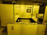
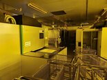
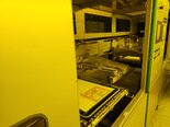
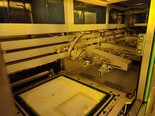
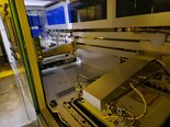
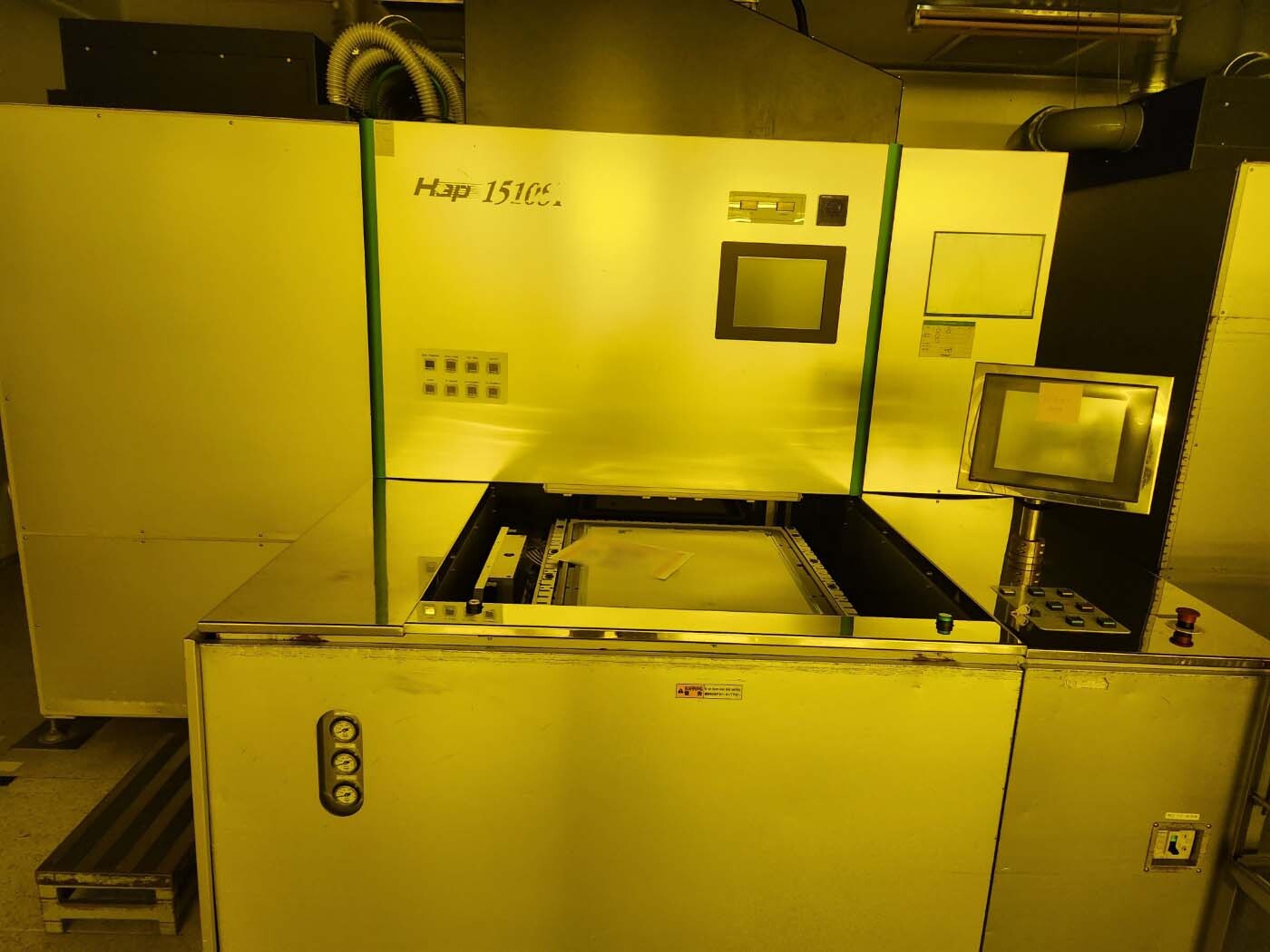
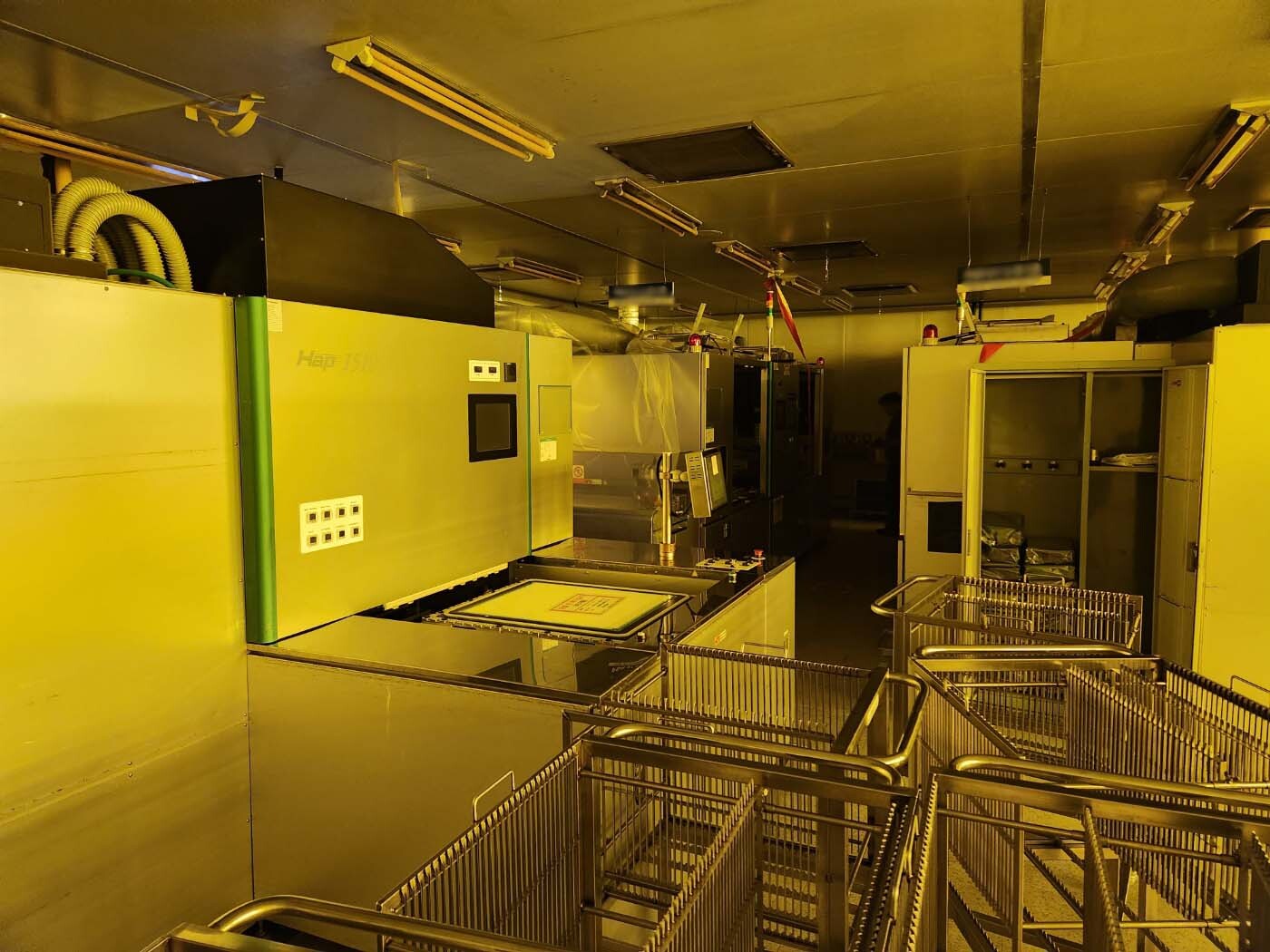
HAKUTO HAP-1510ST is a cutting-edge exposure equipment designed for high-precision lithography processes in the semiconductor and microelectronics industries. As a crucial component in the production of integrated circuits and other electronic devices, HAP-1510ST offers advanced features and capabilities to meet the demanding requirements of modern manufacturing facilities. With a compact footprint and ergonomic design, HAKUTO HAP-1510ST is optimized for efficiency and ease of use in cleanroom environments. The system incorporates state-of-the-art technologies to ensure accurate and reliable exposure of photoresist materials onto silicon wafers with submicron resolution. Equipped with a high-performance projection lens and sophisticated alignment mechanisms, HAP-1510ST enables the patterning of intricate geometries and dense circuit patterns with exceptional clarity and uniformity. One of the key strengths of HAKUTO HAP-1510ST is its versatility and flexibility in accommodating various substrate sizes and types. The unit supports wafer sizes ranging from small pieces to large 300mm wafers, allowing for seamless integration into diverse production processes. Whether manufacturing advanced logic devices, memory modules, or sensor components, HAP-1510ST offers the precision and control required for achieving tight overlay tolerances and critical dimension specifications. The exposure process in HAKUTO HAP-1510ST is controlled with precision through advanced software algorithms and sensor feedback mechanisms. Real-time monitoring and adjustment of exposure parameters such as dose, focus, and alignment ensure optimal performance and consistent results across production runs. The machine's user-friendly interface allows operators to easily configure process recipes, optimize exposure settings, and analyze imaging data for process improvement and yield enhancement. In addition to its exceptional imaging capabilities, HAP-1510ST features advanced automation and robotics for efficient wafer handling and exchange. The tool is equipped with a high-speed wafer loader/unloader and a sophisticated reticle handling mechanism to minimize cycle times and maximize throughput. Integrated sensors and safety interlocks ensure the safe and reliable operation of the asset, supporting 24/7 production schedules with minimal downtime. HAKUTO HAP-1510ST is designed with reliability and serviceability in mind, featuring robust construction and modular components for easy maintenance and troubleshooting. The model's high uptime and low cost of ownership make it a cost-effective solution for high-volume manufacturing environments seeking to achieve production targets with consistent quality and performance. With a comprehensive support network and global service presence, customers can rely on HAKUTO expertise and commitment to customer satisfaction. Overall, HAP-1510ST represents a state-of-the-art exposure equipment that combines precision, versatility, and reliability to meet the evolving demands of the semiconductor industry. With its advanced imaging capabilities, flexible substrate handling, and user-friendly operation, HAKUTO HAP-1510ST is well-suited for a wide range of applications requiring high-resolution patterning and process control. As technology continues to advance, HAP-1510ST remains at the forefront of innovation, empowering manufacturers to push the boundaries of device miniaturization and performance.
There are no reviews yet