Used HAKUTO HAP-5020 #293746362 for sale
URL successfully copied!
Tap to zoom
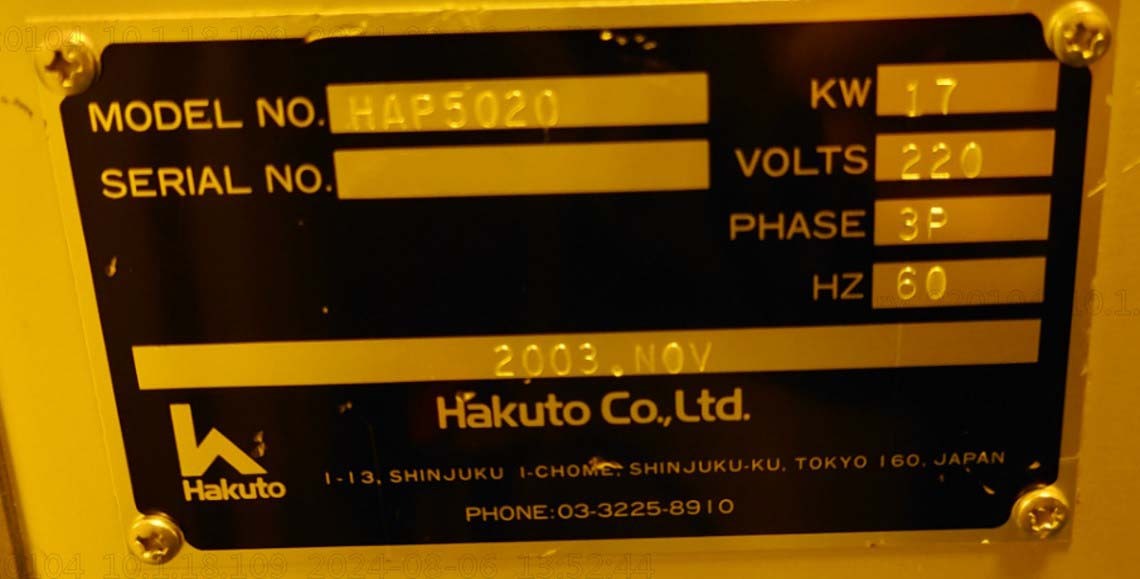

HAKUTO HAP-5020 is an advanced exposure equipment used in the semiconductor industry for photolithography processes. This tool is essential for patterning integrated circuits on silicon wafers, which is a crucial step in semiconductor manufacturing. HAP-5020 is designed to deliver high precision and performance to meet the demanding requirements of semiconductor fabrication. One of the key features of HAKUTO HAP-5020 exposure system is its advanced aligner technology, which enables precise alignment of mask patterns with the wafer surface. This alignment is critical for achieving accurate patterning and ensuring the quality of the final semiconductor devices. The unit utilizes powerful alignment algorithms and high-resolution imaging capabilities to achieve submicron alignment accuracy. HAP-5020 exposure machine also incorporates a sophisticated projection lens tool that enables high-resolution patterning on the wafer surface. The asset utilizes advanced optics and illumination techniques to project the mask patterns onto the photoresist-coated wafer with high fidelity and uniformity. This results in sharp and well-defined features on the wafer, ensuring the integrity of the circuit patterns. In terms of productivity, HAKUTO HAP-5020 exposure model is designed for high throughput and efficiency in semiconductor fabrication. The equipment features fast exposure speeds and automated wafer handling capabilities that enable continuous operation and rapid processing of wafers. This allows semiconductor manufacturers to achieve high levels of productivity and yield in their manufacturing process. Moreover, HAP-5020 exposure system offers flexibility and versatility in patterning various types of semiconductor devices. The unit supports multiple exposure modes, including proximity, projection, and stepper modes, allowing manufacturers to adapt the machine to different process requirements and device designs. This flexibility enables the tool to address a wide range of patterning applications in semiconductor fabrication. Furthermore, HAKUTO HAP-5020 exposure asset is equipped with advanced control and monitoring capabilities to ensure optimal performance and reliability. The model features a user-friendly interface for programming exposure parameters, monitoring equipment status, and analyzing process data. This enables operators to easily set up and control the exposure process, as well as diagnose and troubleshoot any issues that may arise during operation. In conclusion, HAP-5020 exposure system is a cutting-edge tool for semiconductor lithography that offers high precision, performance, and productivity for semiconductor manufacturers. With its advanced aligner technology, projection lens unit, productivity features, flexibility, and control capabilities, HAKUTO HAP-5020 is a versatile and reliable solution for patterning integrated circuits with high accuracy and efficiency. Semiconductor manufacturers can rely on HAP-5020 exposure machine to meet their stringent process requirements and achieve high-quality semiconductor devices.
There are no reviews yet