Used HOYA SCHOTT UL200T-L1 #293774913 for sale
URL successfully copied!
Tap to zoom
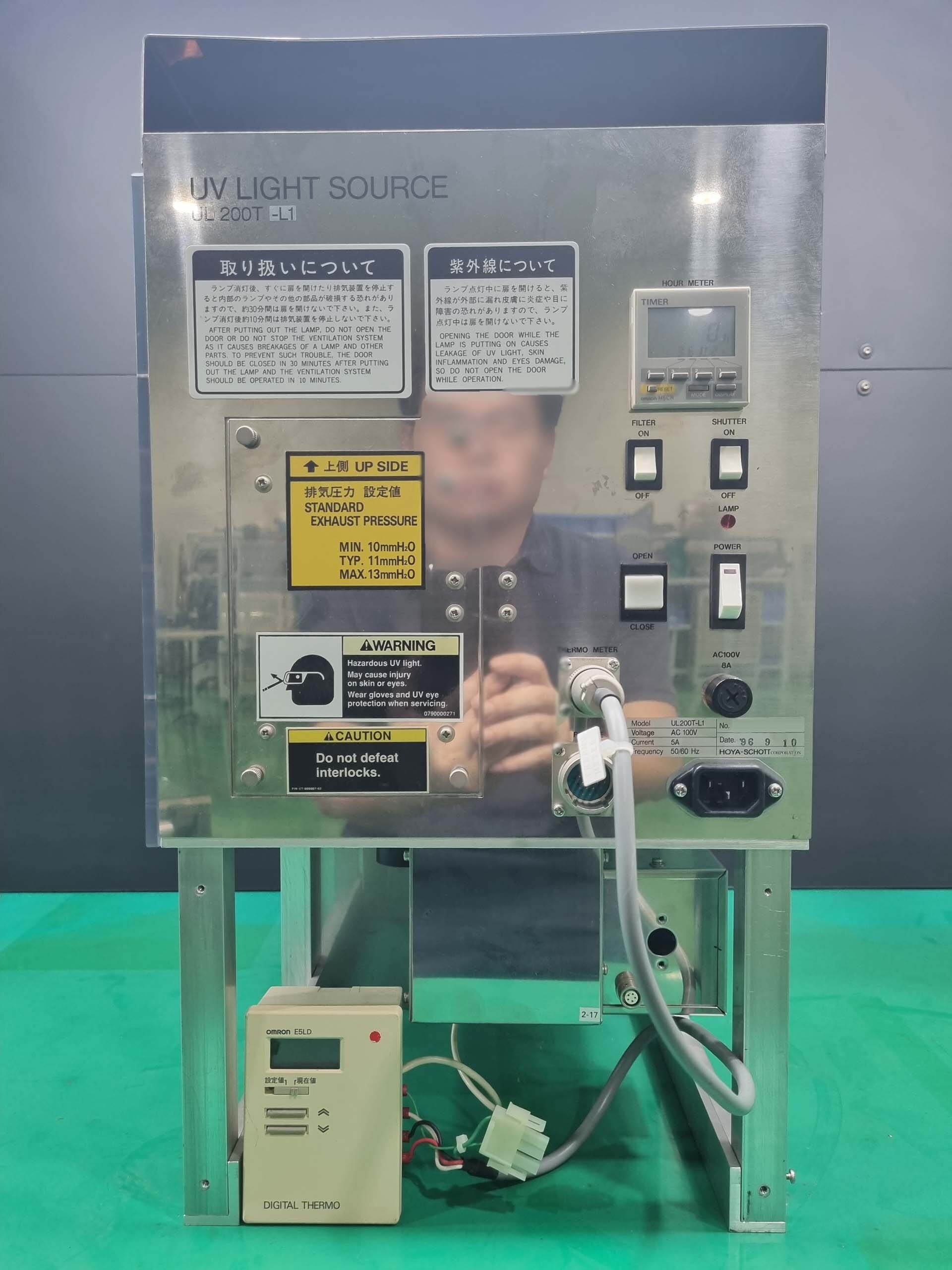

HOYA SCHOTT UL200T-L1 exposure equipment is a cutting-edge technology device used in the semiconductor manufacturing industry for lithography processes. This system plays a crucial role in the production of integrated circuits by providing precise exposure of photoresist materials onto silicon wafers, enabling the creation of intricate microelectronic patterns that form the basis of semiconductor devices. At the heart of UL200T-L1 exposure unit is a sophisticated optical projection machine that utilizes deep ultraviolet (DUV) light sources to project masks containing circuit patterns onto the surface of silicon wafers with exceptional accuracy and resolution. The tool is designed to operate in a controlled environment with ultra-high precision to ensure the optimal transfer of patterns from the mask to the wafer. HOYA SCHOTT UL200T-L1 exposure asset features advanced technology components, including a high-resolution lens model, precision stage mechanisms for wafer positioning, and a robust illumination equipment for uniform distribution of light across the exposure area. These components work in perfect harmony to deliver consistent and reliable exposure results, critical for achieving high yield and quality in semiconductor manufacturing. One of the key highlights of UL200T-L1 exposure system is its ability to support multiple patterning techniques essential for pushing the boundaries of semiconductor device miniaturization. With shrinking feature sizes and increasing complexity in device designs, the unit offers flexibility in patterning strategies, such as multiple exposure and overlay alignment capabilities, to address the challenges of producing next-generation semiconductor devices. Furthermore, HOYA SCHOTT UL200T-L1 exposure machine is equipped with advanced control software that enables real-time monitoring and adjustment of exposure parameters to optimize process performance and ensure high throughput and productivity. The tool's user-friendly interface allows operators to easily configure exposure settings, monitor process status, and analyze data for process optimization and quality control. In terms of performance, UL200T-L1 exposure asset delivers exceptional resolution capability, with the ability to achieve sub-micron feature sizes required for advanced semiconductor nodes. The model's high throughput capability enables rapid exposure of multiple wafers in a production environment, maximizing fab productivity and efficiency. Additionally, HOYA SCHOTT UL200T-L1 exposure equipment is designed for reliability and robustness, with built-in features for system maintenance, calibration, and diagnostics to ensure continuous operation and minimal downtime. The unit's modular design facilitates ease of servicing and upgrades, making it a cost-effective investment for semiconductor manufacturers looking to stay competitive in the ever-evolving semiconductor industry. In conclusion, UL200T-L1 exposure machine represents a state-of-the-art solution for semiconductor lithography applications, offering unparalleled precision, flexibility, and performance to meet the demanding requirements of modern semiconductor manufacturing. With its advanced technology features and robust design, HOYA SCHOTT UL200T-L1 exposure tool is a vital tool for driving innovation and enabling the production of cutting-edge semiconductor devices that power the future of electronics.
There are no reviews yet