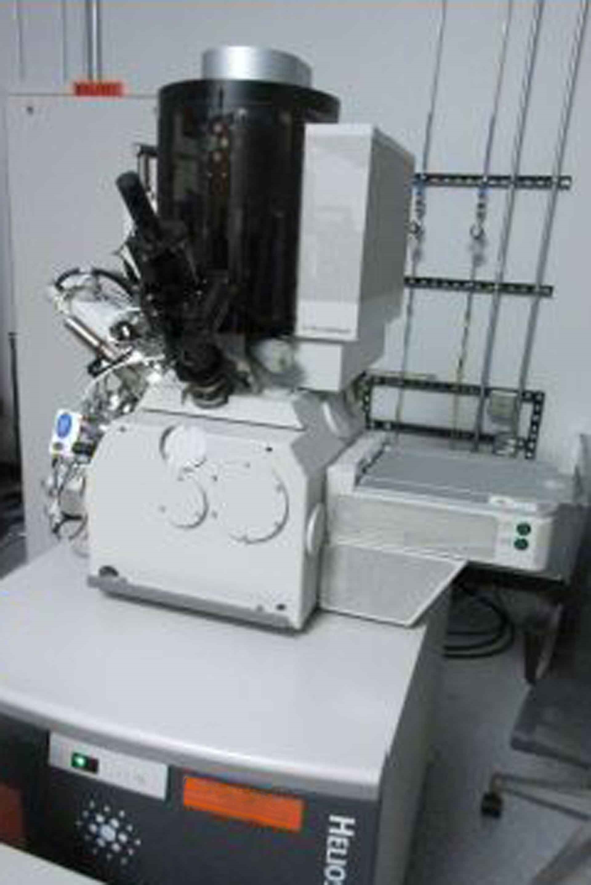
Used FEI Helios NanoLab 400 #9232837 for sale
It looks like this item has already been sold. Check similar products below or contact us and our experienced team will find it for you.
Tap to zoom


Sold
FEI Helios NanoLab 400 is a Focused Ion Beam (FIB) equipment optimized for nanoscale milling, deposition and imaging applications. It is an integrated, Field Emission Gun (FEG) based system used for the controlled growth of thin films, low-k dielectric materials and nanostructures. The unit combines an inert gas milling gun, equipped with a high-speed motor, with a milling chamber that is temperature-controlled for optimal process results. Helios NanoLab 400 offers a high degree of control for producing objects and features with a wide range of dimensions. The machine enables the fabrication of nanostructures in a broad range of materials, such as metals, semiconductors, polymers and dielectrics. Its probe current range is adjustable from 0.1 pA to 400 nA, allowing for high-resolution imaging with a lateral resolution of less than 10 nm. FEI Helios NanoLab 400 is equipped with high-resolution imaging optics, including an electron beam (EB) microscope, a secondary electron detector (SED) and a aperture detector (AD). The EB gun has a maximum accelerating voltage of 20 kV and can detect large-angle and small-angle scattered electrons. The SED is made of an aluminum plate, which can be used for backscattered electron, secondary electron and transmitted electrons imaging. Finally, the AD provides the capability for low-angle imaging, with a field of view up to 0.5 μm. Helios NanoLab 400 delivers advanced features for nanofabrication, such as directional milling. With a dynamic range up to 500 keV, the milling gun enables the acquisition of high-resolution, nanoscale images of inner structures which are not accessible to conventional imaging techniques. This capability is especially useful for milling through complex three-dimensional features of components, such as integrated circuits, with a high degree of precision and accuracy. FEI Helios NanoLab 400 also provides advanced capabilities in thin film deposition and deposition metrology. On-stage heating, dual heating settings and automated thin-film thickness mapping are all available, making it possible to accurately control the location and thickness of thin films during the deposition process. The tool also supports a range of multi-functional deposition processes, such as conformal coating, atomic layer deposition and electro-stitch. Helios NanoLab 400 provides an efficient, versatile platform for nanofabrication, thin film deposition and metrology. Its combination of high-resolution imaging, directional milling capabilities and thin-film deposition enable the production of high-quality components and features with maximum process precision and control.
There are no reviews yet