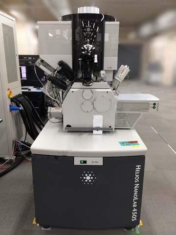
Used FEI Helios NanoLab 450S #9268041 for sale
It looks like this item has already been sold. Check similar products below or contact us and our experienced team will find it for you.
Tap to zoom


Sold
ID: 9268041
Focused Ion Beam (FIB) system
Electron source: SCHOTTKY Thermal field emitter
STEM Resolution: 0.8 nm
Ion source: Gallium liquid metal
Running hours: 1,000
Landing voltage:
SEM: 50 V - 30 kV
FIB: 500 V - 30 kV
SEM Resolution:
Optimal WD:
0.8 nm at 15 kV
0.8 nm at 2 kV
0.9 nm at 1 kV
1.5 nm at 200 V With beam declaration
Coincident WD:
0.8 nm at 15 kV
0.9 nm at 5 kV
1.2 nm at 1 kV
Ion beam resolution at coincident point:
Preferred statistical method: 4.5 nm at 30 kV
Selective edge method: 2.5 nm at 30 kV
Stage:
Flipstage with in-situ STEM detector
OMNIPROBE Sample extractor
5-Axis piezo motorized
XY Motion: 100 mm
Loadlock: Maximum 80 mm diameter
Sample types:
Wafer pieces
TEM
Grids
Whole wafers: Up to 100 mm
User interface:
Windows GUI with integrated SEM
FIB
Gas Injection System (GIS)
Patterning
Imaging mode
Detectors: ETD, TLD, ICE
Chamber 1: Carbon C10H8
Chamber 2: Tungsten W(CO)6
Chamber 3: Platinum C5H4CH3Pt(CH3)3
Remote components:
NESLAB ThermoFlex900 chiller
XDS10i Pre vacuum pump
ONEAC Transformer: 200V AC, Single phase
APCO UPS: 100V AC, Single phase
EDS Resolution: <30 nm on Thinned samples
Does not include Hard Disk Drive (HDD).
FEI Helios NanoLab 450S is an ion milling equipment that offers unsurpassed performance for precision sample preparation. This system is designed to allow researchers to produce the highest quality samples for scanning electron microscopy (SEM) and transmission electron microscopy (TEM). It is an ideal choice for preparing samples for imaging, analysis, and device fabrication. The NanoLab 450S utilizes a unique combination of ion milling and lithographic techniques to create precise patterns, electric structures, and mechanical features on the surfaces of samples. The ion milling process is highly controlled, allowing researchers to produce uniform and repeatable results. The 360-degree rotating sample holder allows users to optimize the angle of the ion beam for the best results. The unit features a high-powered dual-ion beam machine that supports multiple base voltages (15-30 kV) and beam energies (1-10 keV). The dual ion beams allow researchers to etch through complex structures and prepare oddly shaped features. In addition, the dual ion beams produce less heat than traditional ion milling systems, allowing users to quickly and accurately prepare samples for both SEM and TEM. The tool is equipped with a state-of-the-art ContolPix™ automated patterning asset, which automates pattern definition, mask creation, exposure, and ion milling, allowing users to quickly and accurately replicate patterns or define their own custom masks. The model also supports a variety of lithography techniques, including multi-level double exposure for 3D structures and nanolithography. The NanoLab 450S offers a wide range of options for controlling the ion beam current and etch rate to ensure the best possible results. In addition, the equipment is designed to reduce vibration to help maintain the precision of the etching results. The NanoLab 450S also features advanced monitoring and control functions, ensuring that the process is as safe and controlled as possible. Helios NanoLab 450S is a cutting-edge, highly precise ion milling system that offers unparalleled performance for sample preparation. With its powerful dual-ion beam unit, automated patterning machine, and advanced monitoring and control functions, the NanoLab 450S is an excellent choice for researchers looking to produce the highest quality imaging, analysis, and device fabrication samples.
There are no reviews yet