Used MICROBEAM Nanofab 150 #9032282 for sale
URL successfully copied!
Tap to zoom


ID: 9032282
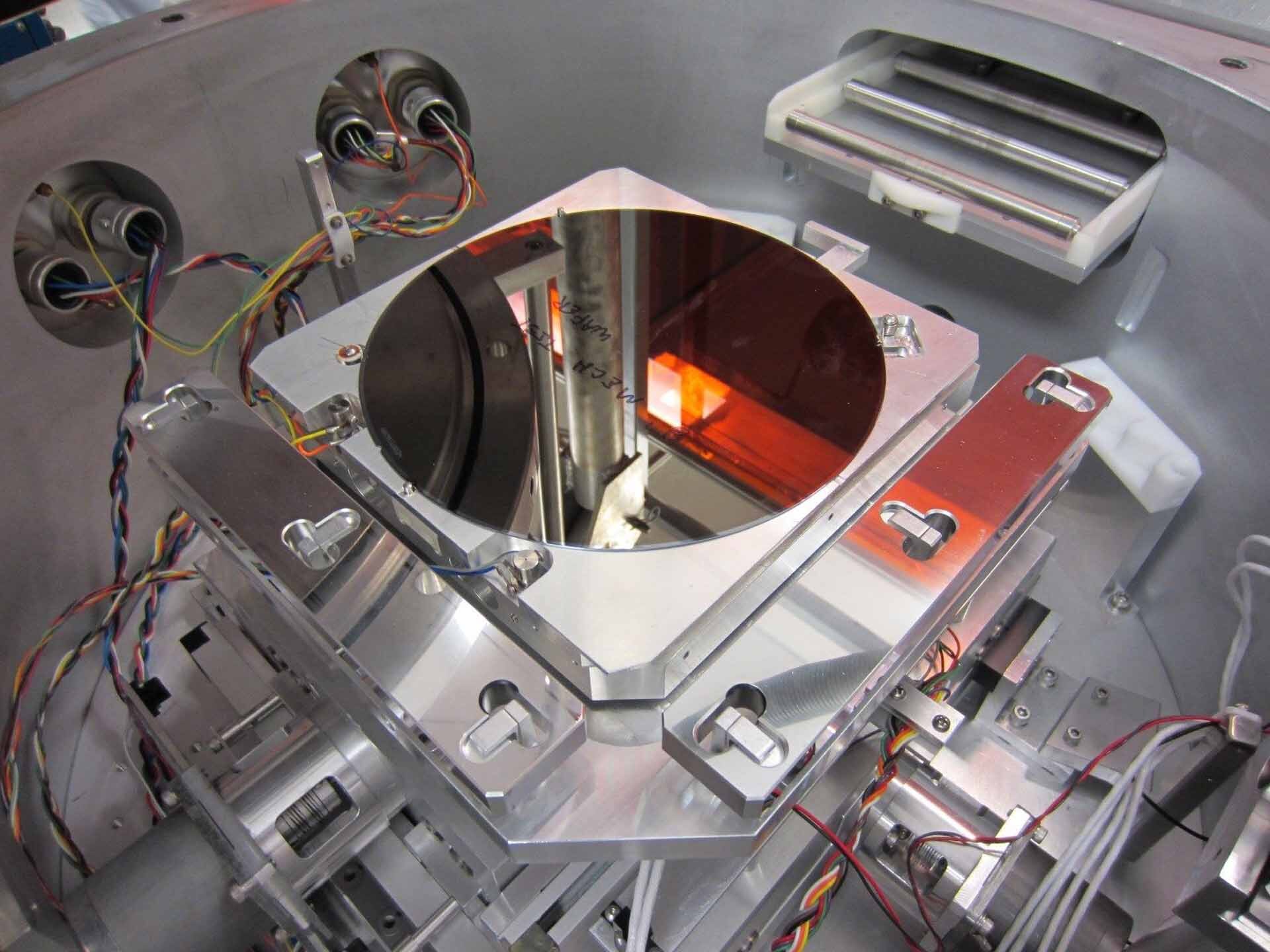
Wafer Size: 6"
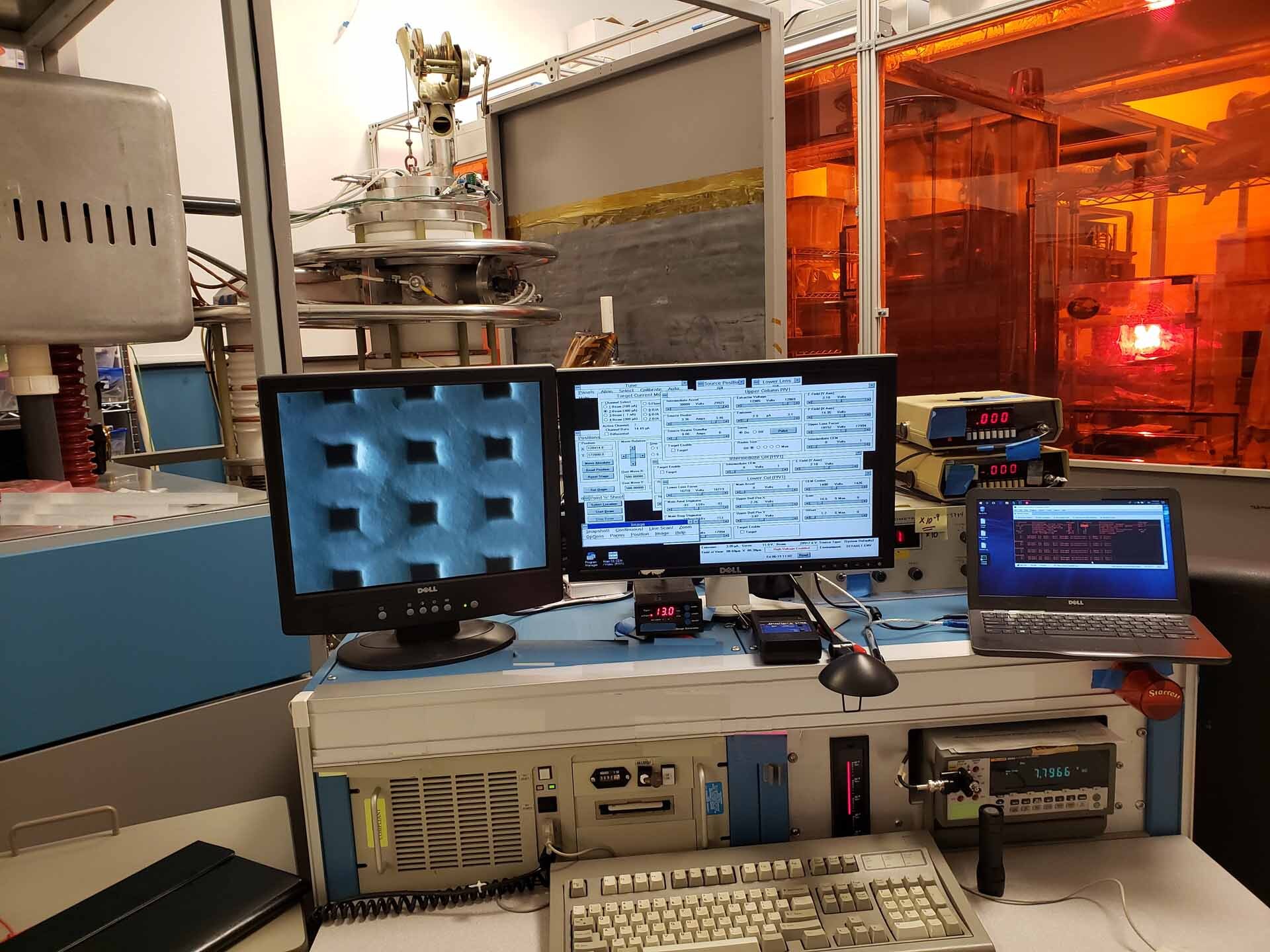
Direct write ion beam lithography system, 6"
GDSII
Integrated laser position stage
Minimal beam spot size: 20nm
Energy: 4 -150 keV (300 keV double ionization)
ExB Mass filter
M/deltaM ≥ 50
Liquid metal ion sources: Ga, Si, Ge, In, Be, Au, As, B, Pd, Bi
Beam current density: Up to 5A/cm2
Computer controlled
Stepper motor driven substrate state: 165mm x 165mm travel
1 nm Resolution laser position monitor
Upgrade options available:
Advanced sub 10nm ion optics
Stainless steel system with 10 Pallet load-lock (6" wafer only)
8" wafer handling (2 pallet load-lock only)
General System Upgrade (GSU): Includes vacuum, computer, data handling software, interferometer
Ion sources: 5A/cm Ga, Si, Ge, In, Be, Au, As, B, Pd, Bi sources
Ion guns
Advanced Performance Gun (APG) and source.
MICROBEAM Nanofab 150 is an ion milling equipment used to create precise and intricate features into surfaces of thin films and substrate materials evenly. It utilizes an ion beam milling process- also known as ion beam etching- which uses an ion beam to physical ablate the existing material or thin film. The system works by introducing a high intensity beam of ions, generally Argon, at a substrate material at a low pressure atmosphere. The ions travel in an arc from the source to the electrode at a determined voltage. The ions, when they collide with the material, rip off electrons and thus ablate the material evenly or with some predetermined patterns according to the user settings. The particles and material vapor created by the bombardment are then drawn away from the unit by a vacuum pump, ensuring no potential damage to the substrate material. The machine's main advantages over other milling processes are its high precision, flexibility in the choice of sources, and its capacity to ablate many different substrate materials. The degree of precision that can be achieved through the use of this tool is particularly useful for critical materials or for the production of features with complex shapes. Furthermore, depending on the settings, the user can also determine the level of uniformity of the ablation with a certain degree of accuracy. For instance, the user can choose different parameters such as the ion energy or dose depending on the size and shape of the feature required. As such, the asset can be used to create features of different shapes, such as rectangular, circular, conical or even honeycomb patterns, as well as textures of various sizes. Nanofab 150 model provides users with a highly efficient and precise way to etch substrates and thin films with utmost precision and accuracy. This equipment is extremely flexible and customizable, allowing users to control the speed, ion energy and power to ensure an accurately milled surface. Furthermore, its high precision makes it ideal for use in critical materials and the production of complex, intricate features.
There are no reviews yet

