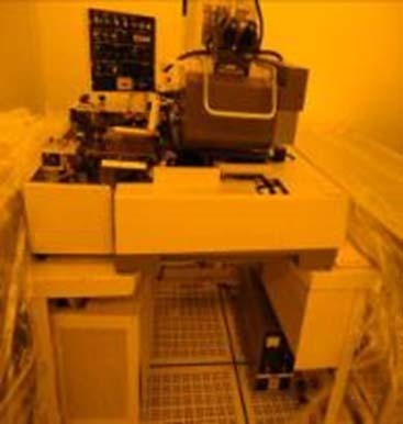
Used CANON PLA 501 FA #9328963 for sale
URL successfully copied!
Tap to zoom


ID: 9328963
Wafer Size: 5"
Mask aligner, 5"
Gases:
N2:
Maximum pressure: 3.5 kg/cm²
Maximum flow: 10 LPM
Pipe: SUS316
Connector: SWAG
Caliber inch: 1/4"
CDA
Vacuum
Mercury lamp: 250 W
Wafer exposure, 5"
Ground: 1 ohm
Manual included
Power supply: 220 V, Single phase, 3-wires, 1.6 A
Lamp power supply: 110 V, Single phase, 3-wires, 5.5 A.
CANON PLA 501 FA is a mask aligner designed for use in nanometer-scale optoelectronic device fabrication applications, such as those involving light-emitting diodes (LEDs), lasers, and photovoltaics (PVs). It is a versatile machine which can be used to precisely align to high-resolution patterns in photomasks, as well as to align organic materials and etch them into desired shapes. CANON PLA-501FA utilizes a combination of mechanical and optical components for superior accuracy and precision in the alignment and overlay processes. It includes a high-precision, motor-driven x-y stage for aligning the mask on the substrate, and a laser diode light source for detecting the edge and overlay of the photomasks. A CCD imaging device allows the operator to perform alignment, overlay, and etching operations with ease. In addition to the imaging capabilities, the machine is equipped with a pair of vacuum chucks that allow the operator to secure the substrate on the x-y stage and an adjustable height free-space alignment package that allows for the exact positioning of the photomask. PLA 501FA offers high-resolution patterns through its 0.35 μm scanner and is capable of scanning at 1.5 m/s. It also features an optical zoom that allows for magnification factors of up to 1,000X, which enables precise alignment and etching operations. Finally, the machine is equipped with calibration and test charts that enable the user to ensure that the machine is operating accurately and at the correct resolution. PLA-501FA is an excellent choice for optoelectronic device fabrication applications. Its combination of precision, speed, and accuracy makes it particularly well-suited for the demanding process of creating nanometer-scale devices. Its versatility also allows it to be used for a range of other applications as well, such as micro-etching and the fabrication of organic and inorganic materials.
There are no reviews yet

