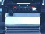
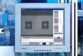
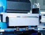
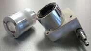
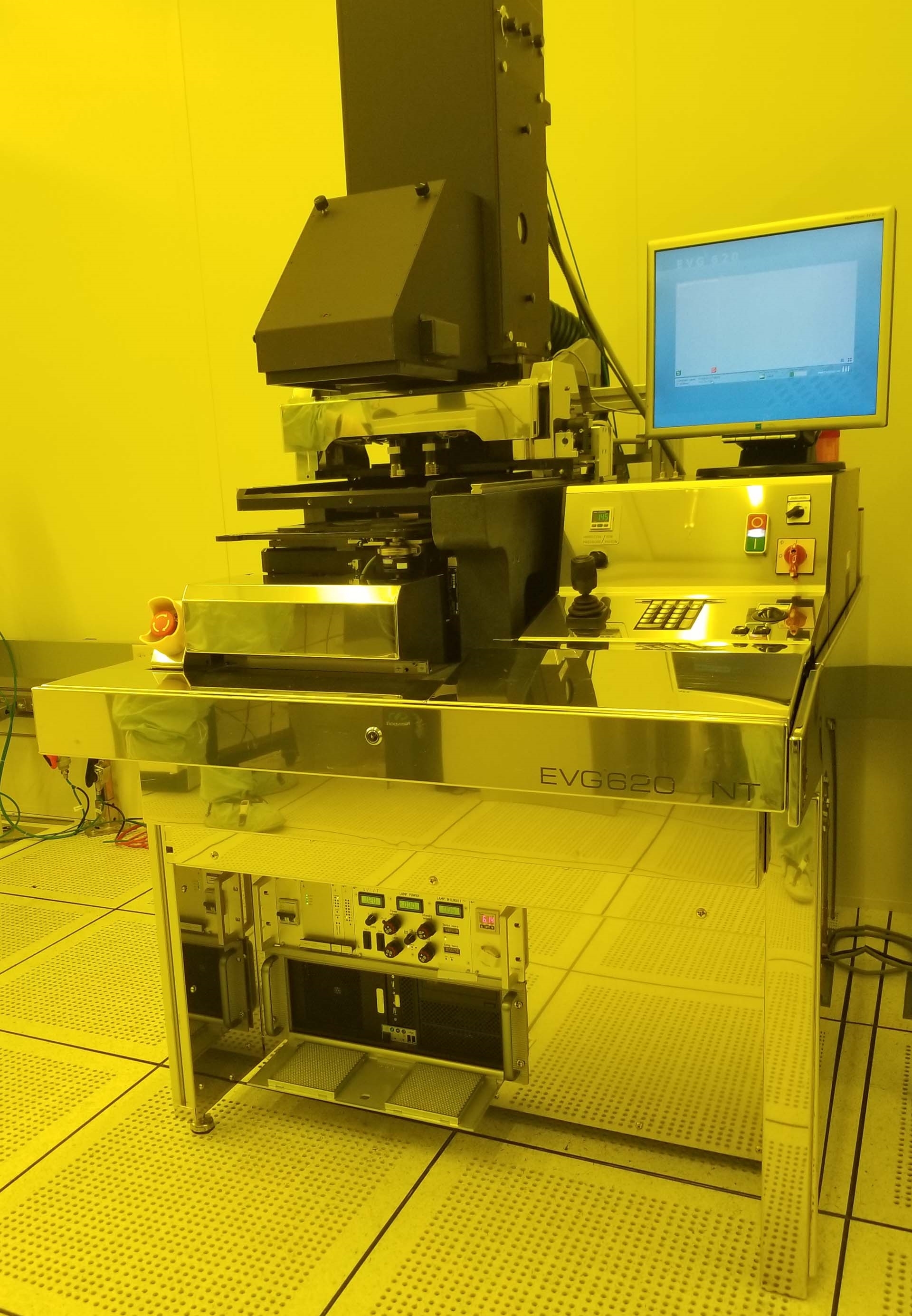
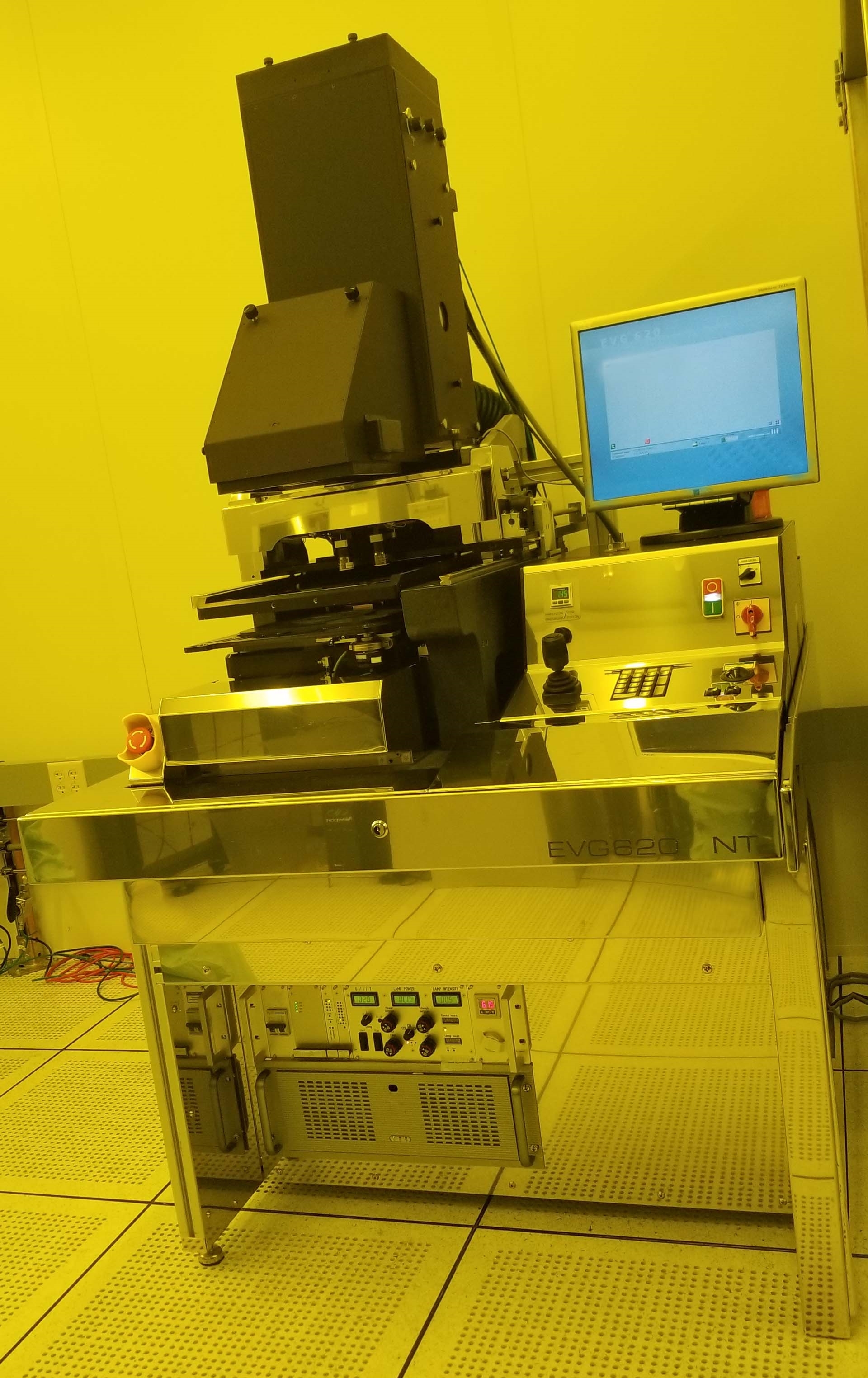
Used EVG / EV GROUP 620NT #9191006 for sale
URL successfully copied!
Tap to zoom













ID: 9191006
Wafer Size: 6"
Vintage: 2011
Automated double side lithography system, 6"
Exposure modes:
Hard
Soft
Vacuum contact
Proximity
Separation distance: 0-300 μm adjustable
Wafer thickness: 0.1-10 mm (For top side configuration only)
Semi automatic loading
Mechanical pre-alignment on chuck
Quick change of mask and chuck
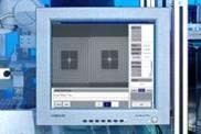
Flat screen for operator interface and alignment functions, 17"
PC Controlled operating environment
Granite base frame construction
Active vibration isolation
Password protected access levels:
Operator
Engineer
Maintenance
Back side alignment of wafers:
Mounted carrier
Deep etched back side alignment marks
Supports measuring of structures
Cross hair distance
Resolution with 10x objectives: 1.1 μm
Light source NUV: 500 W-1000 W
Lamp house: 350 W / 500 W Hg lamp
Optical sets in NUV range: 280-450 nm
Optimized parallel light:
±2%, 4"
±3%, 6"
UV Probes:
Diameter: 44.5 mm
Height: 16 mm
Optical set for wave length: 350 nm-450 nm
Light sources: NUV / DUV
Field lens, 6"
Dielectric mirror
Fly's eye lens
Alignment stage fully motorized
Fully motorized X, Y, Theta & Z alignment stage
With DC motor controllers
Automatic wedge compensation system
Optimized print gap control
WEC Contact force: 0.5-40 N adjustable
Top side microscope:
Motorized split field microscopes in visible light
With high resolution CCD cameras for top and bottom side
Travel range:
X: 30 (8)-150 mm
Y: -70 / +70 mm
Storage of objective positions
Digital zoom: 2x / 4x
Image magnification for fine alignment
(2) Objectives: 10x (3.6x - 20x)
Bottom side microscope:
Motorized split field microscopes in visible light
With high resolution CCD cameras
Bottom side alignment
Travel range:
X: 68 (48) mm-150 mm
Y: ± 12 mm
Digital zoom: 2x / 4x
Image magnification fine alignment with objectives
(2) Objectives: 10x (3.6x - 20x)
Rack unit EVG 620 mask aligner systems:
Integrates EVG 620 desktop alignment system
Vibration isolated
Robotic auto load system
Robot module for auto load cassette to cassette:
Size: 4"-6"
With non contact optical prealigner for wafers
With flat and notch
Standard: With vacuum from bottom side
Robot control fully integrated to EVG 620
Graphical User Interface (GUI)
Cassette station:
Send
Receive
Standby
(5) Cassette stations:
Cassette present sensor
Cassette empty sensor
Semi standard wafer cassette sizes
IR Light source: Bottom side objectives
IR-Transparent substrates
Bottom side microscope: IR Light source manipulation
IR Alignment of wafer to mask using top side microscope
IR Lamp position with recipe
Active cooled IR light source
Manual and automatic alignment processes
Usage of special IR objectives on topside microscope
Reduces bottom side microscope travel range
Pick and place handling option:
Programmable send / receive / standby cassette configurations
Up to 75 wafer processing on handling modules:
(3) Cassette stations
No operator intervention
125 wafer processing on handling modules:
With (5) cassette stations
No operator intervention
Hard UV-Nano imprinting:
UV-NIL Processes with hard stamps (Quartz glass)
Top chuck, 1" stamps (in diameter)
Bottom chuck:
Microscope slides:
10 x 10 mm
15 x 15 mm
25 x 75 mm
Diameter: 2"-4"
Soft UV-NIL and μ-CP:
PDMS Stamp to be mounted on glass back plane (5" square)
Bottom chuck, 4"
Loading frame, 1" Stamp
Contact free wedge compensation with spacers
Adjustable contact force for vacuum printing process
Top chuck with quartz windows for UV curing of resist
Optical alignment of stamp and substrate in two steps:
Separation of stamp and substrate: Rough alignment
Soft contact of stamp: Fine alignment
Vacuum contact: 100 - 850 mbar
Mask holder for 5" x 5" masks with loading frame
Bottom loading system
with automated vacuum transfer
Hard coated & lapped surface finish for mask contact area
Mask holder for 7" x 7" masks with loading frame
Bottom loading system with automated vacuum transfer
Hard coated & lapped surface finish for mask contact area
Universal wafer chuck, 4"
With spacers
For automated handling
Hard coated & lapped surface finish for wafer contact area
Universal wafer chuck, 6"
With spacers
For automated handling
Hard coated & lapped surface finish for wafer contact area
Manual filter changing unit without filter / carrier
Includes:
Bond alignment
Signal tower
Does not include cassette load
2011 vintage.
EVG / EV GROUP 620NT is a mask aligner designed to support advanced ionizing radiation (e-beam) and optical lithography requirements in semiconductor fabrication and other industries. Its aligner provides precise alignment of photomask patterns to the wafer surface, ensuring accurate replication of features and uniformity of performance of the device. EVG 620NT features an advanced two-beam equipment, which enables targeting and positioning of a wide range of patterns with subpixel accuracy and rock-solid stability. Its wide-angle optics provide unmatched field of view and allows alignment of large areas of patterns in one go. In addition, the system provides an efficient working environment with a modern GUI and several tools for easy operation, including robotics for handling of mask and wafer. The performance of theEVG EV GROUP 620NT is further enhanced by its high-resolution imaging unit, which features a 12k x 12k-pixel CCD area scan camera that captures images using nanometer-level resolution. An integrated micron-level auto stage is capable of providing tight registration accuracy and repeatability, so patterns can be positioned within a single-digit nanometer accuracy over the entire field of view. 620NT is built with expandable modular components, which allows users to easily upgrade or modify the equipment when needed. Innovative architecture and dedicated data communication lines offer extremely fast imaging, with scan speeds of up to 10 megapixels per second. To keep up with the rapid changes in device manufacturing, further advances in the imaging machine are possible with an upgradeable hardware platform. EVG / EV GROUP 620NT is a powerful and reliable tool for those involved in the challenging task of creating and replicating advanced semiconductor features. Its combination of cutting edge optics, high precision imaging, rock solid platform, and upgradable hardware ensures an efficient working experience and a uniform, defect-free performance of the device.
There are no reviews yet


