Used KARL SUSS / MICROTEC MA-150 CC #9249160 for sale
URL successfully copied!
Tap to zoom
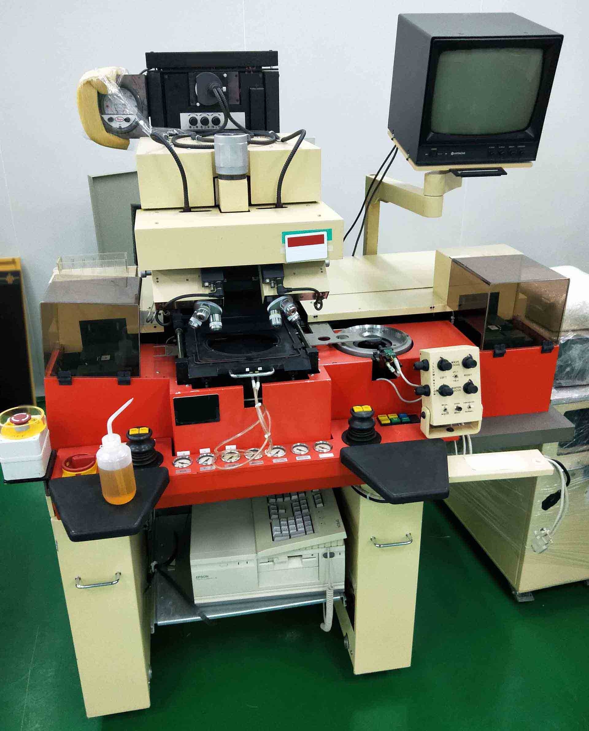

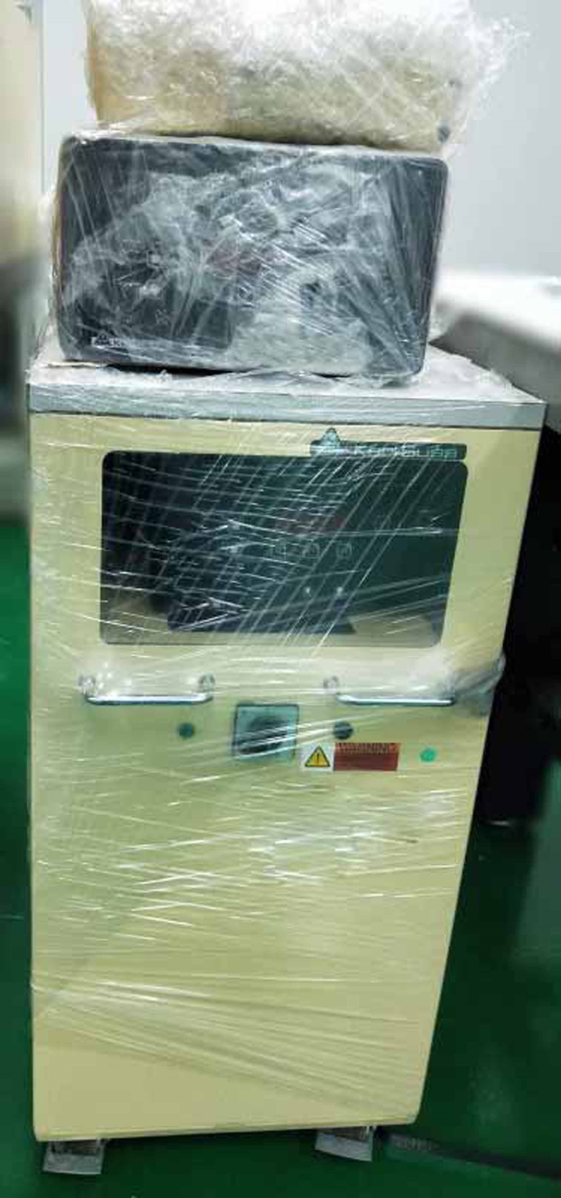

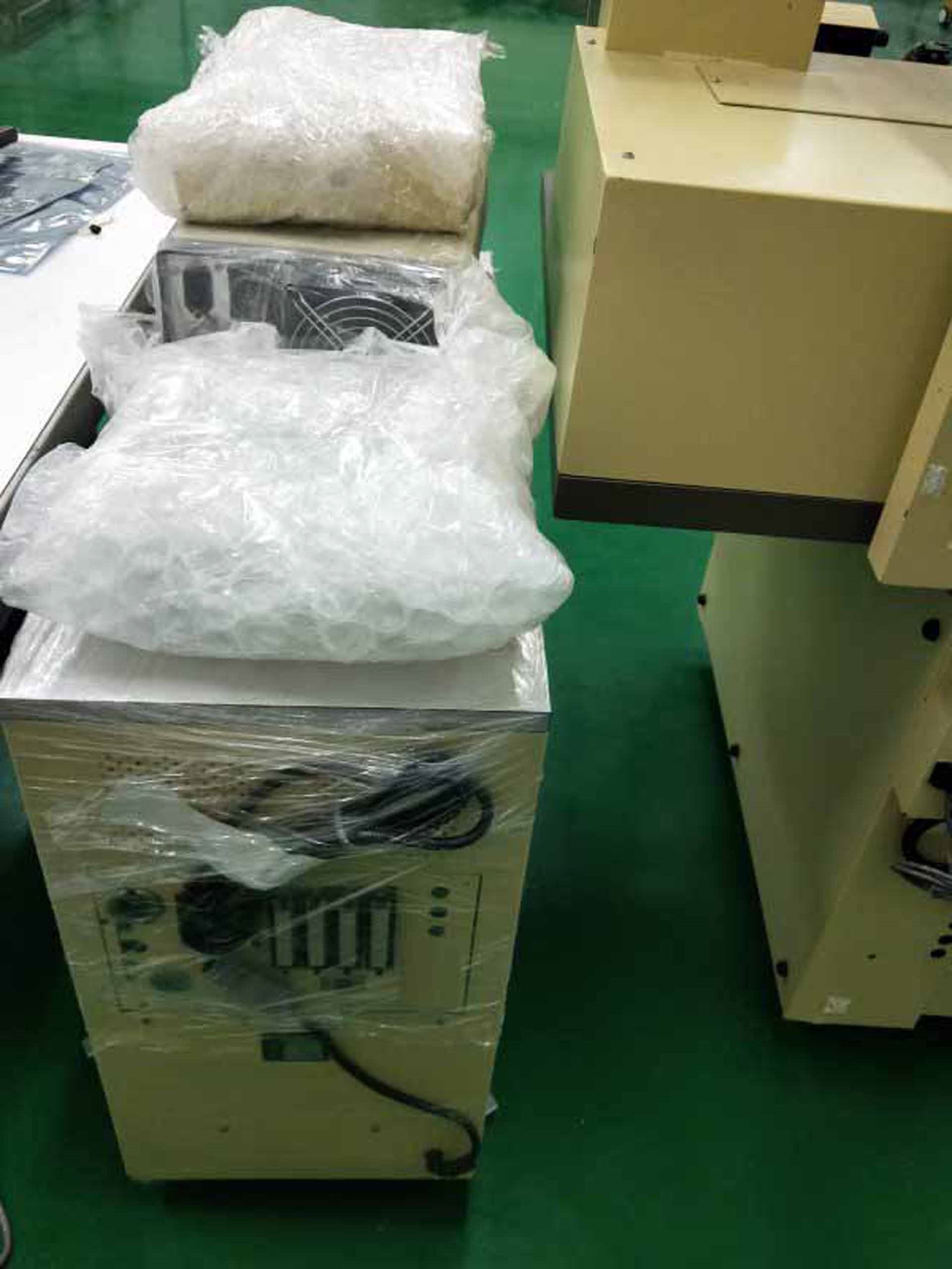

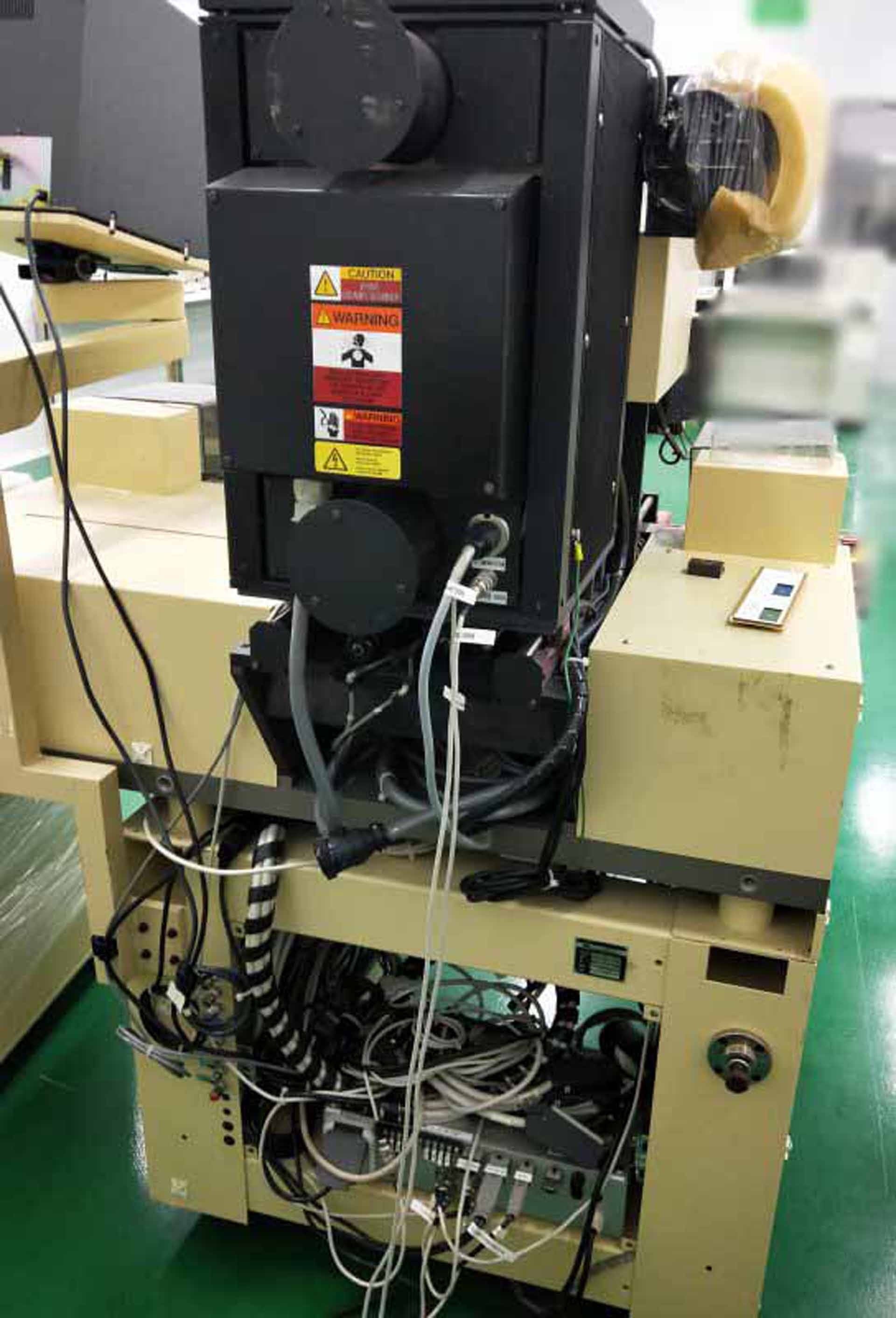


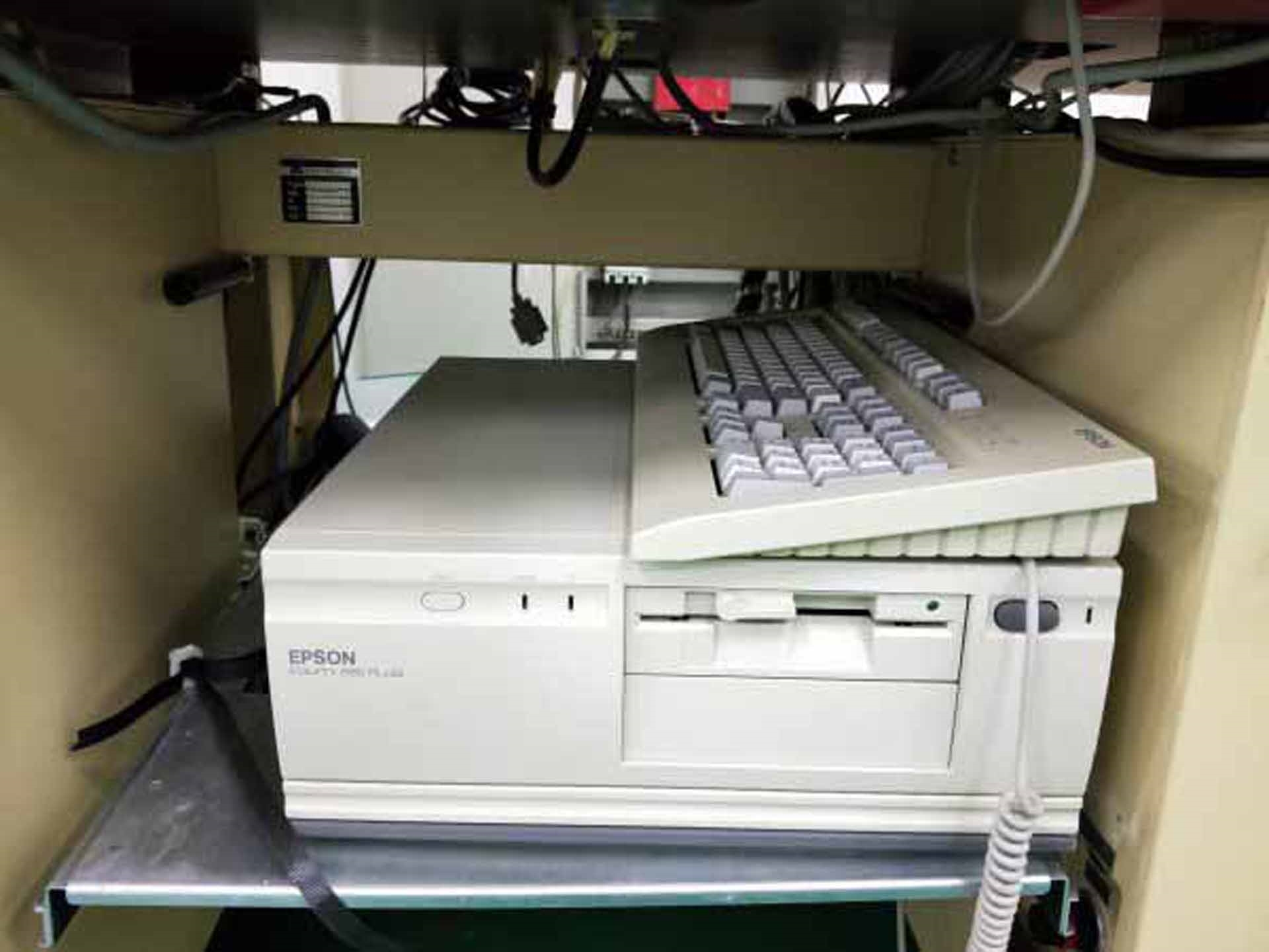

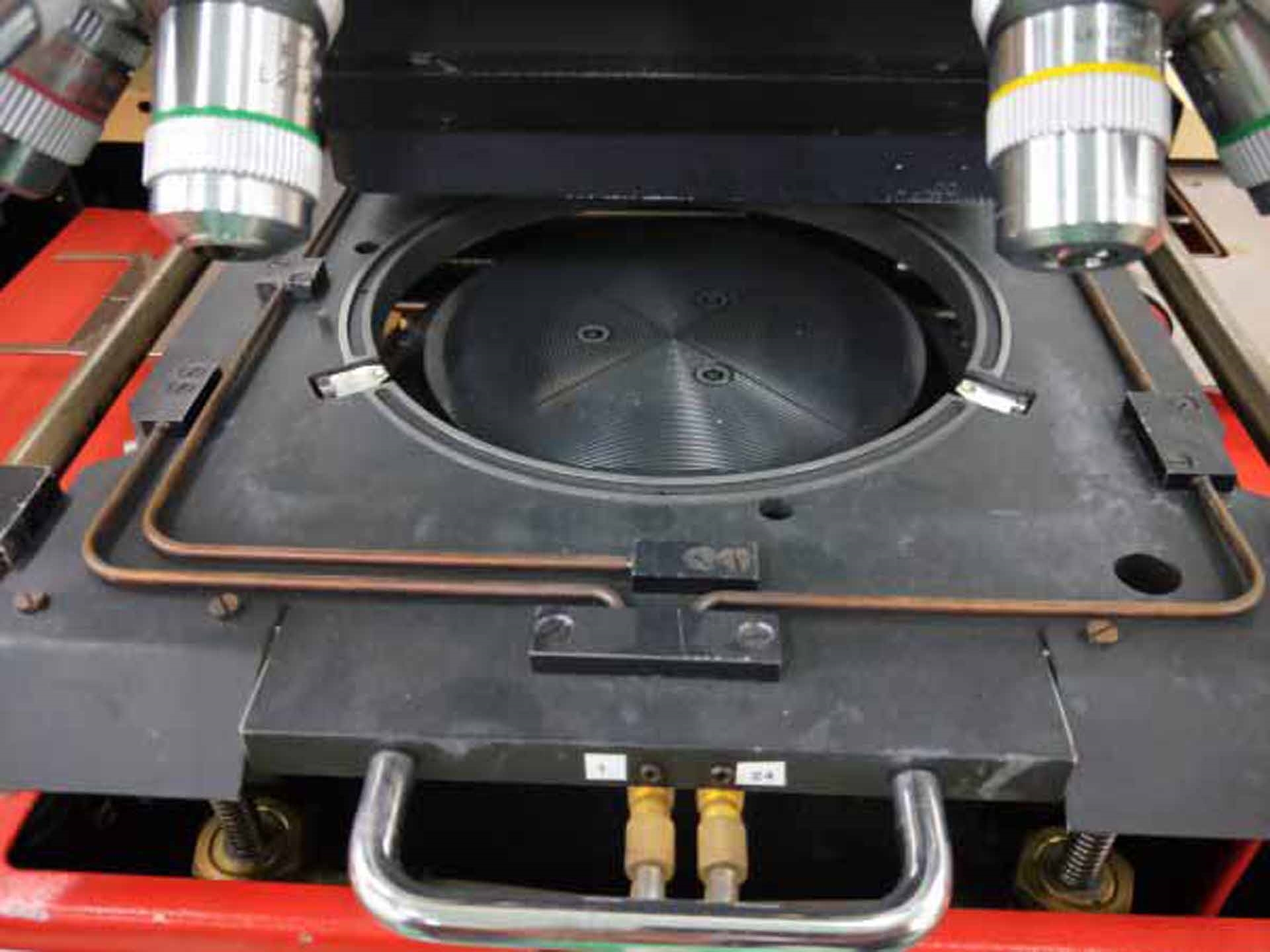


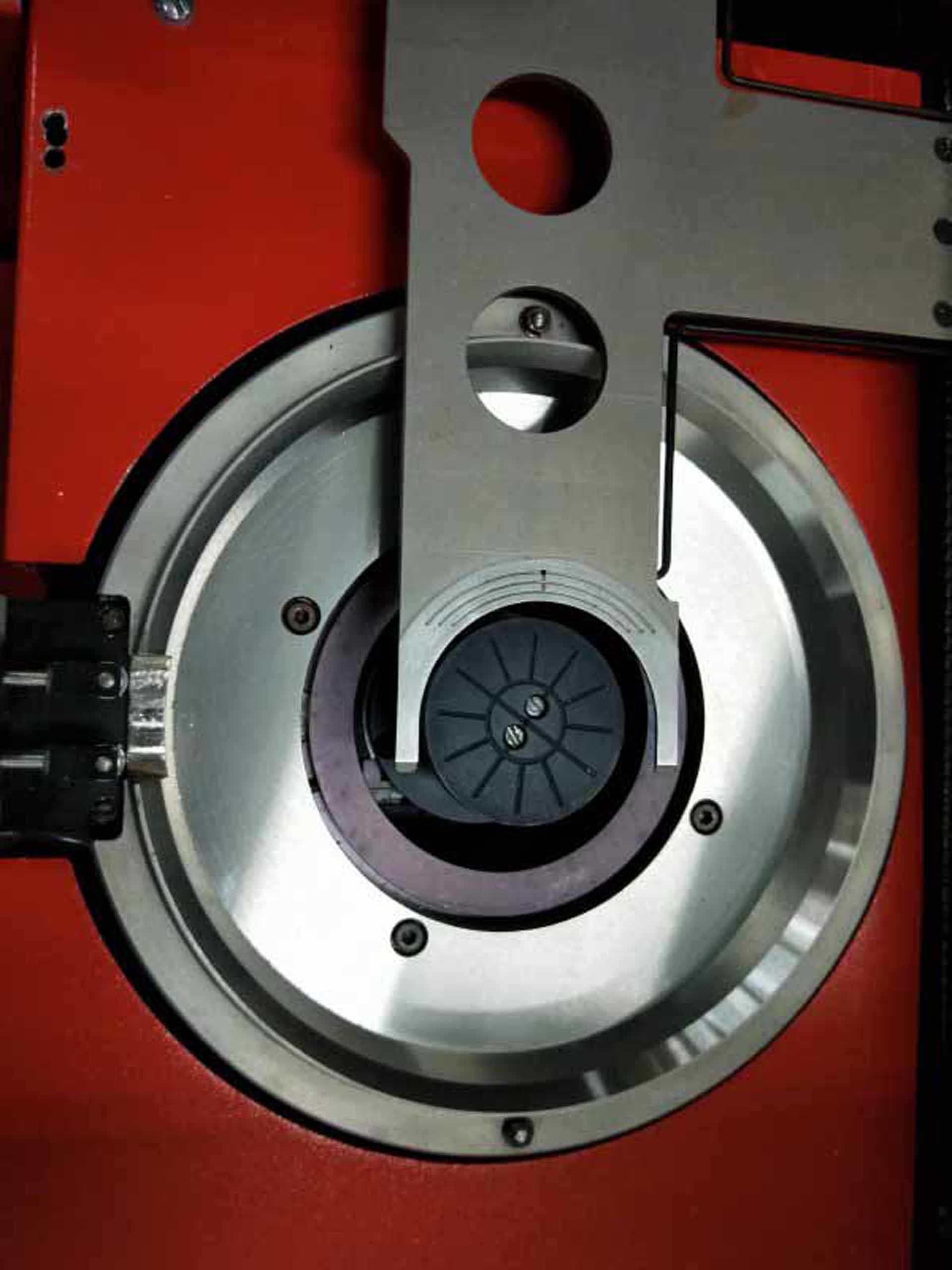

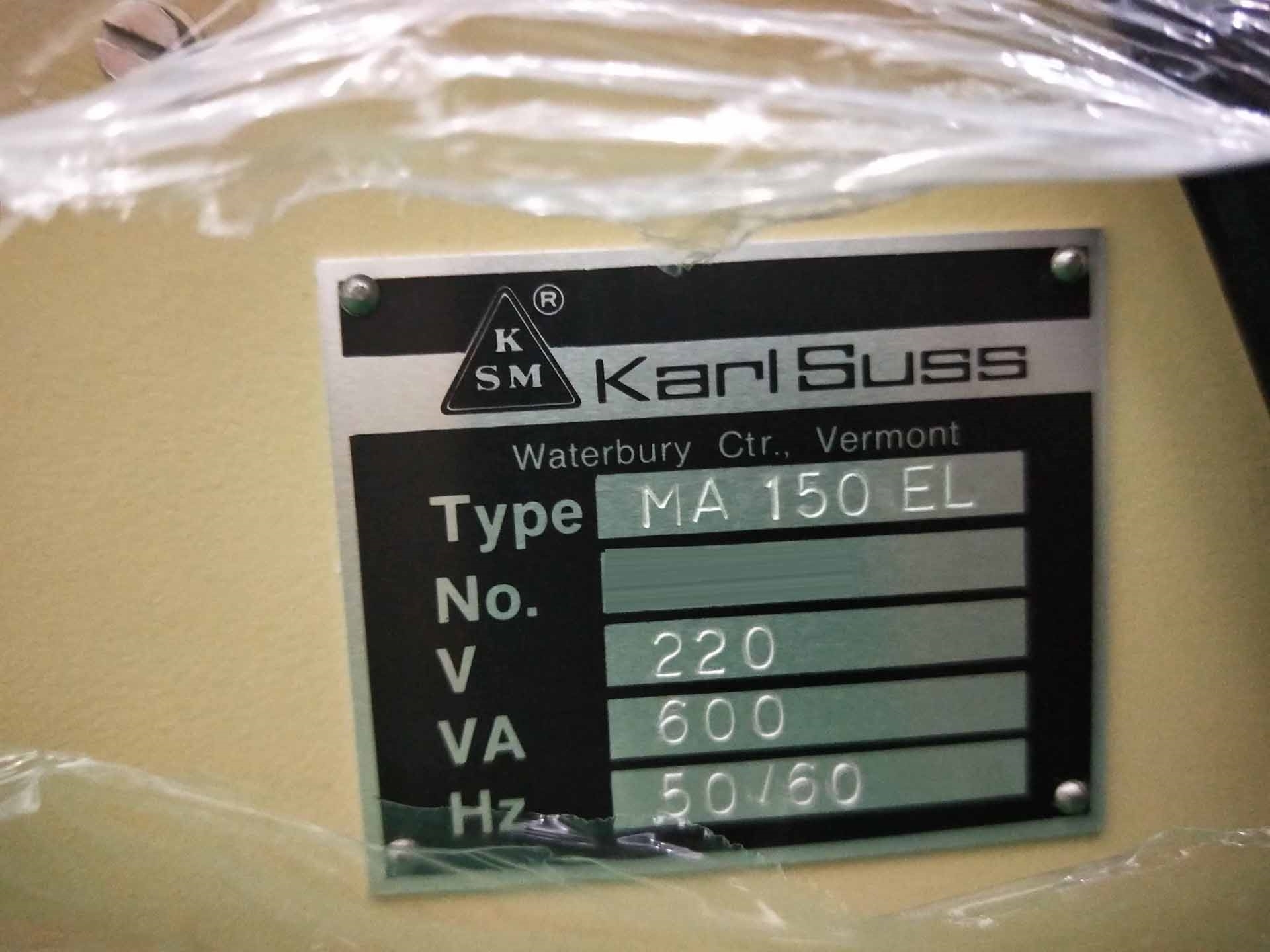

KARL SUSS / MICROTEC MA-150 CC Mask Aligner is a highly efficient, accurate, and robust lithography system ideal for producing sub-micron features and structures on wafer surfaces. Utilizing an electrically charged beam of electrons, the aligner is capable of precisely positioning, centering, and exposing semi-conductor layers with a high accuracy and resolution. The aligner features a loading mechanism that securely holds and aligns wafers while they are being processed, as well as a process control module that allows for fine-tuned adjustments to ensure optimal lithographic processes. MICROTEC MA150CC aligner supports a range of common and specialized processes, including contact photolithography and deep UV projection, due to its excellent energy shielding. Additionally, KARL SUSS MA 150CC allows for manual stepper travel distances of up to 25mm and step resolutions of 1µm in the X, Y, and Z directions enabling large-scale production. The aligner also includes an alignment and registration camera that captures images of wafer patterns and provides feedback for correction and alignment of each incoming wafer. Furthermore, MICROTEC proprietary smart process recipes software allows for reliable and efficient alignment of over 20 processing parameters. For high-precision performance, MA150CC aligner is equipped with a solid-state shutter, active thermal control, and high-capacitance storage. The shutter ensures crisp alignment of patterns while eliminating the need for delicate film resins. Additionally, the aligner features an active thermal control system that facilitates consistent temperature throughout production; this ensures long-term pattern-alignment reliability and superior results. Finally, MICROTEC MA-150 CC's high-capacitance storage maintains vital parameters and control settings even when the main power is suspended. In short, MICROTEC MA-150CC Mask Aligner is a top-of-the-line system for producing low-distortion, high-precision wafer patterns and structures.
There are no reviews yet


