Used OAI J500 #293810208 for sale
URL successfully copied!
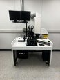
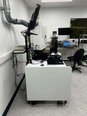
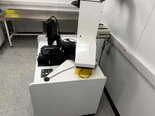
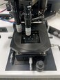
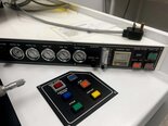
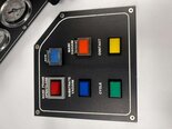
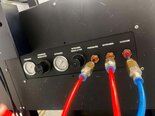
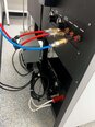

Tap to zoom
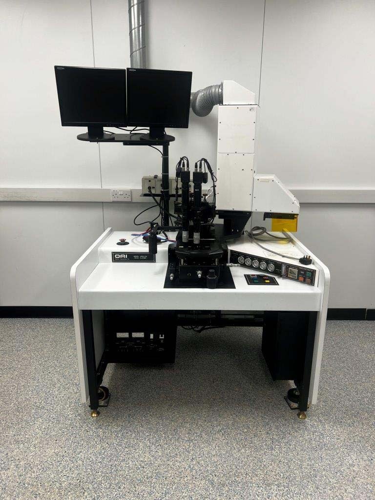

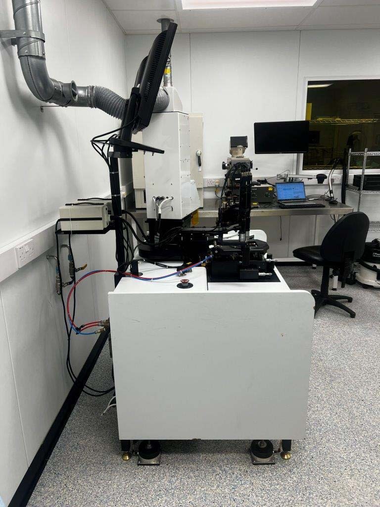
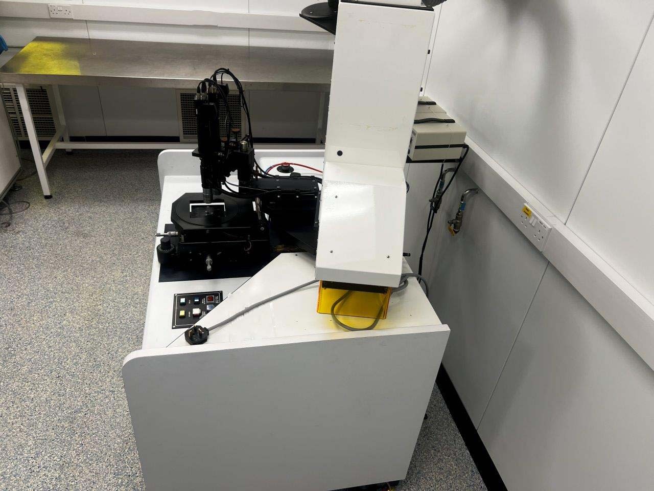
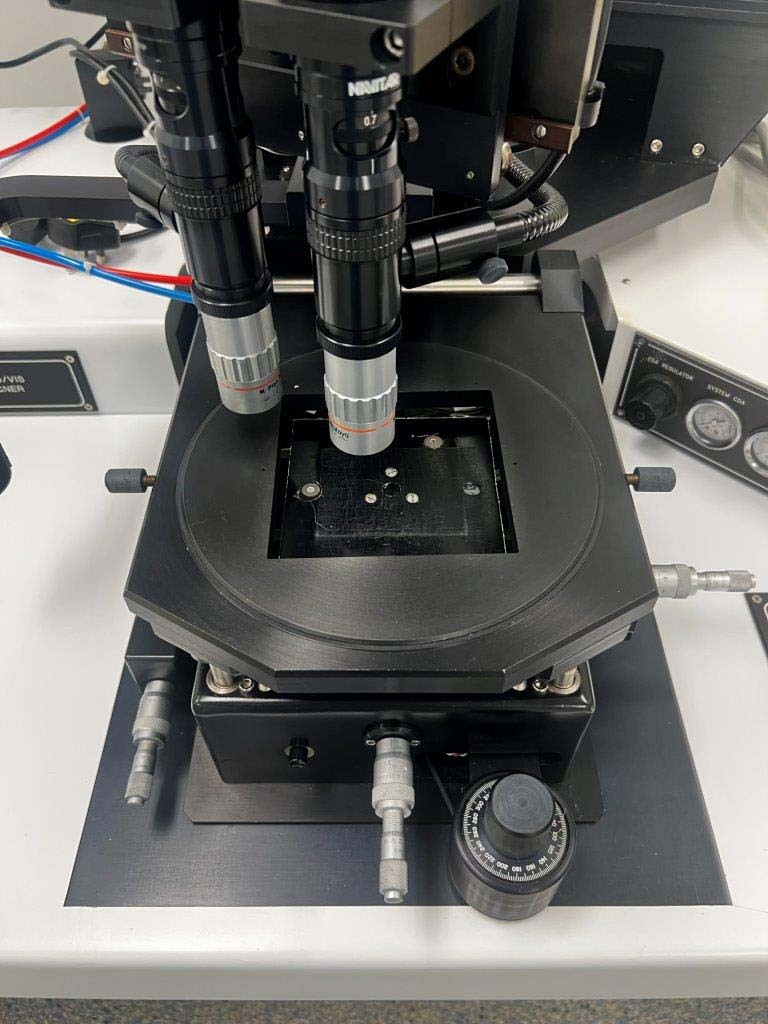
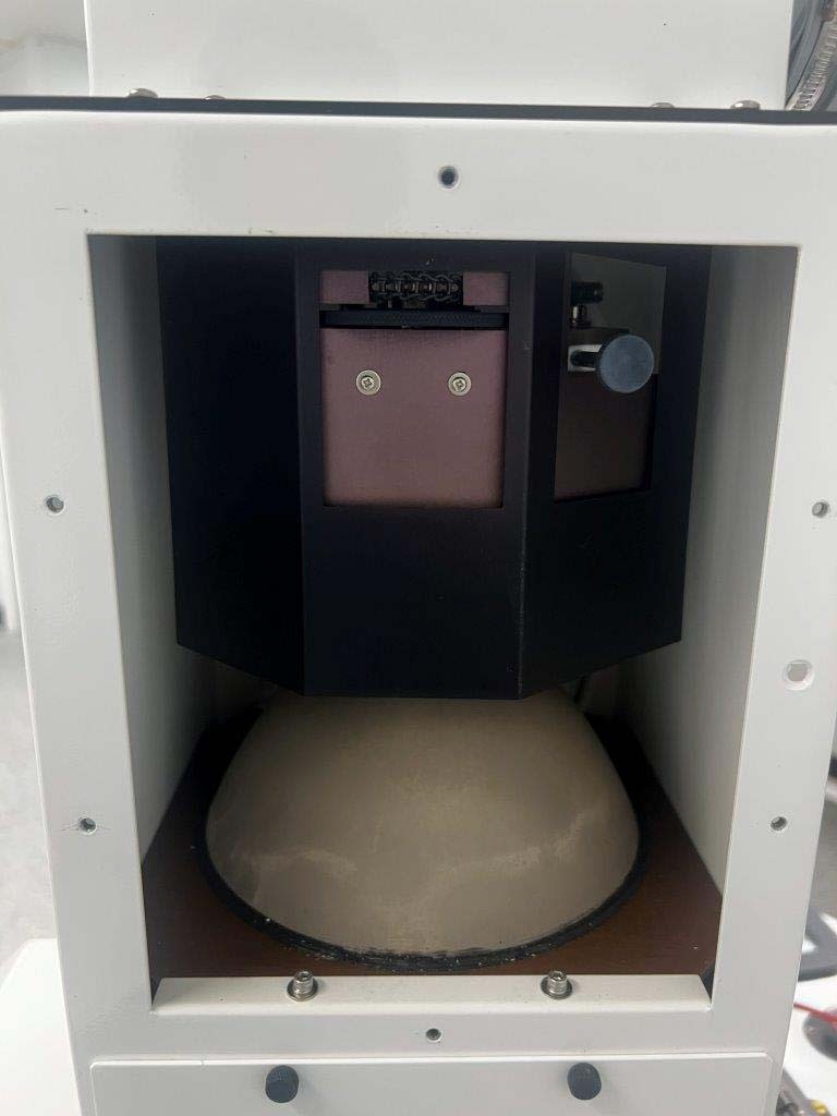
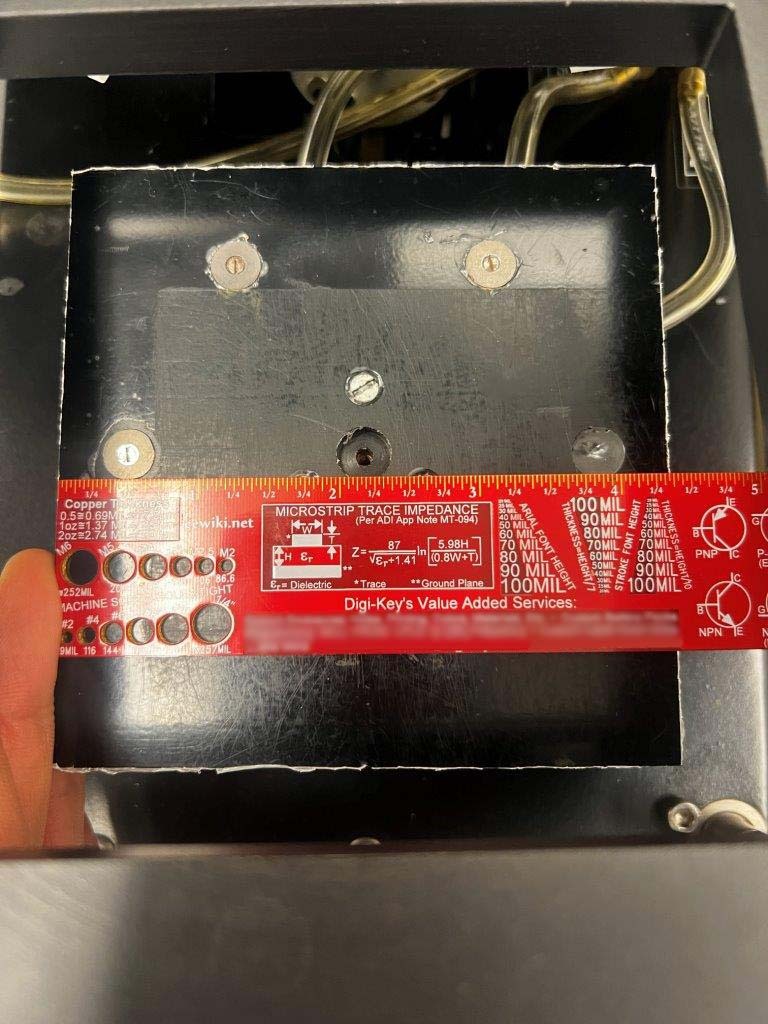
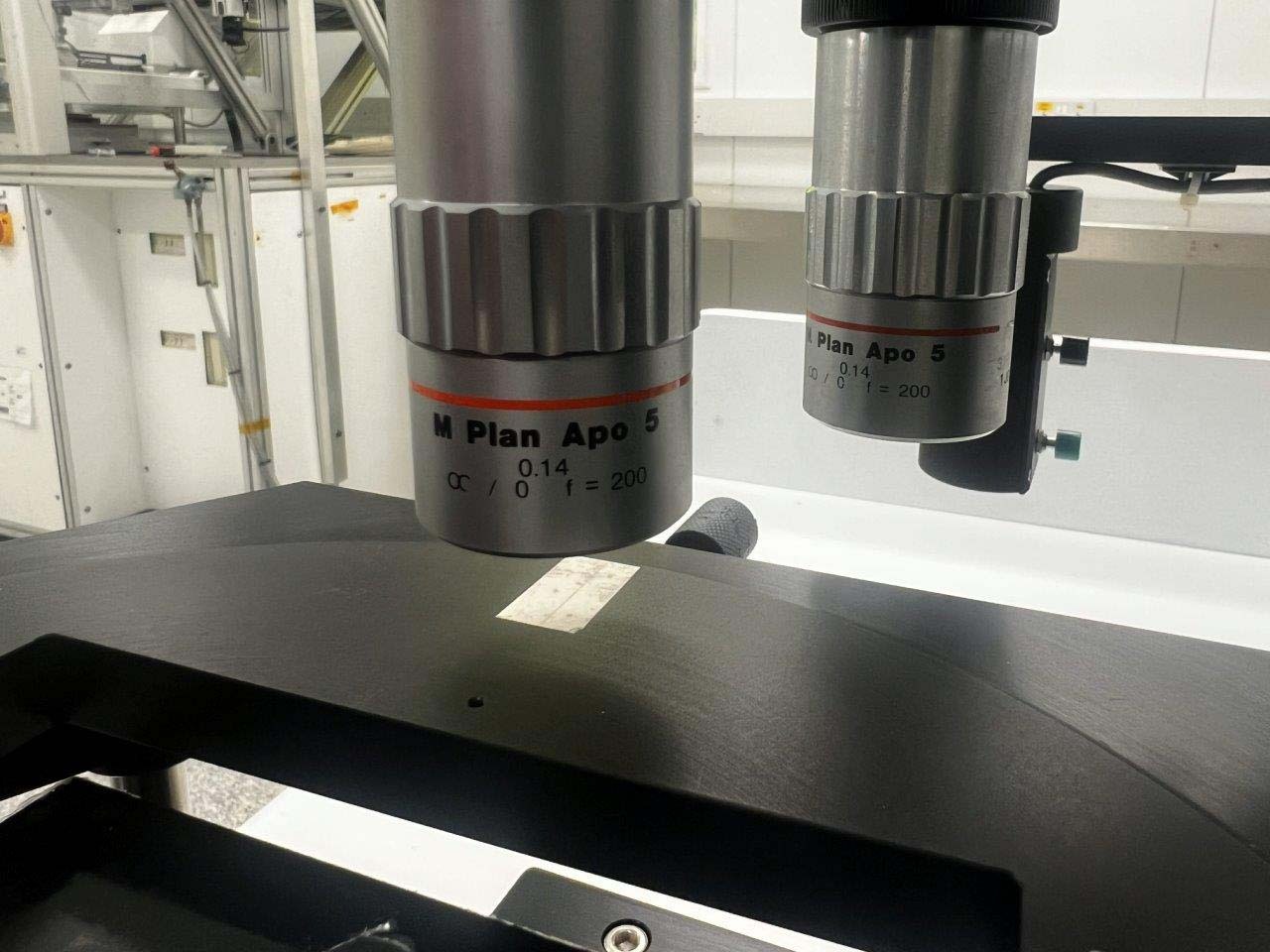
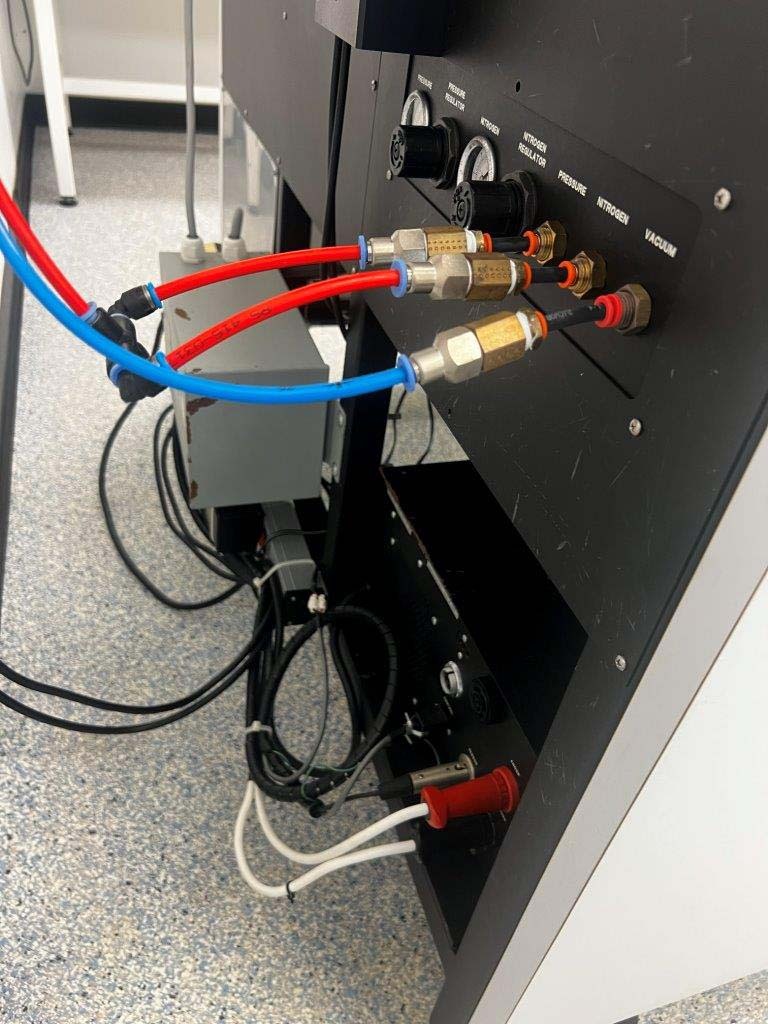
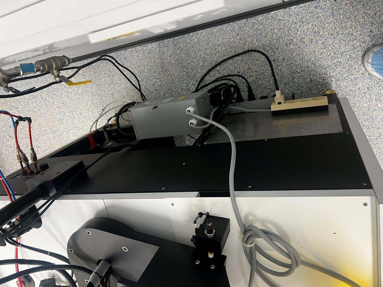
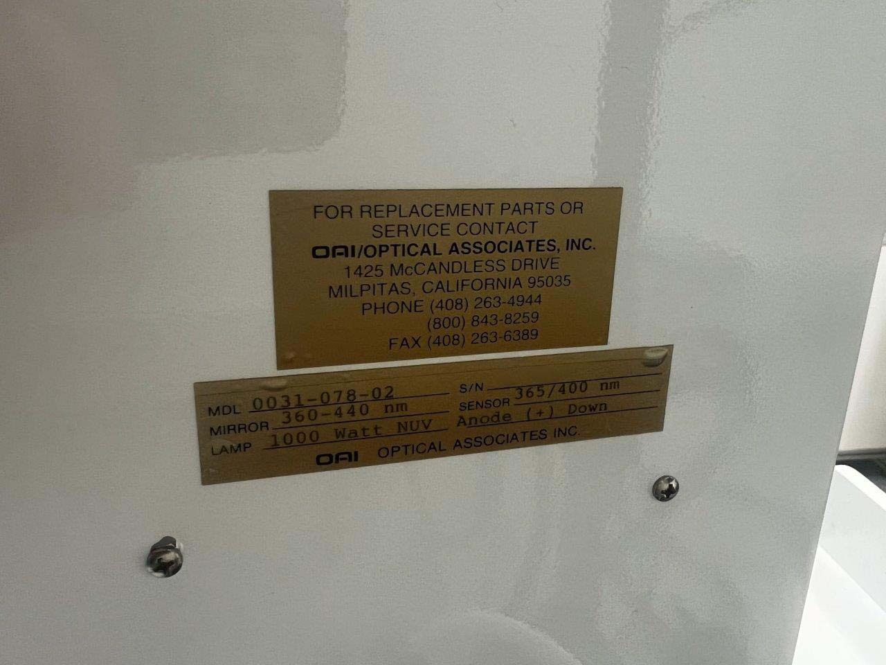
ID: 293810208
Wafer Size: 8"
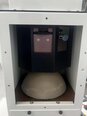
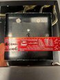
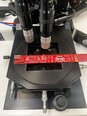
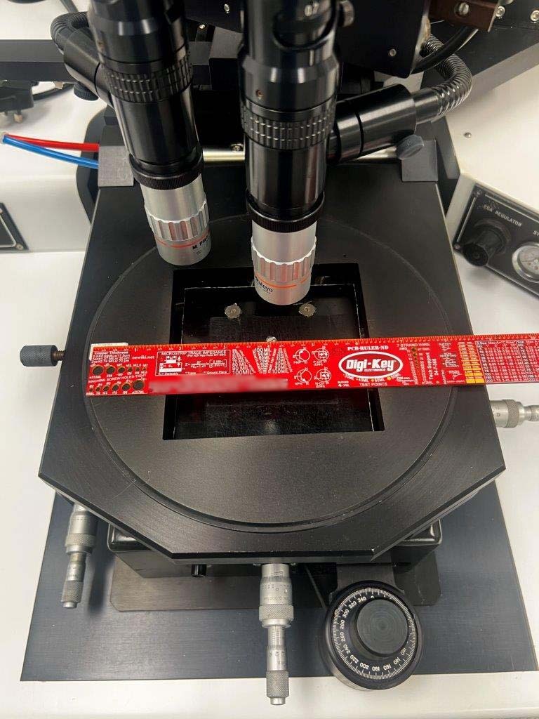
Mask aligner, 8"
Lamp house: 360-440 nm
Wavelength: 1Kw NUV, 365/400 nm sensor
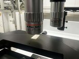
NAVITAR Adjustable optics
PULNIX 7CN Camera
MITUTOYO Lens
Mask frame size: 4"-5"
UV Lamp: 1000W NUV.
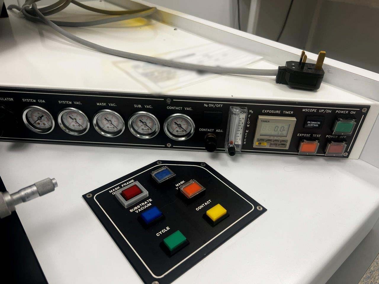
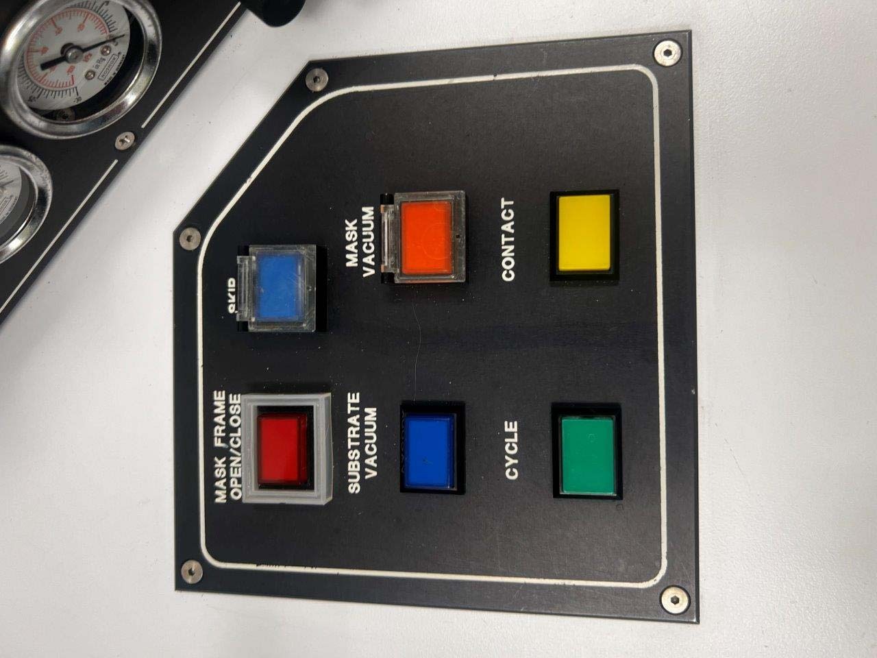
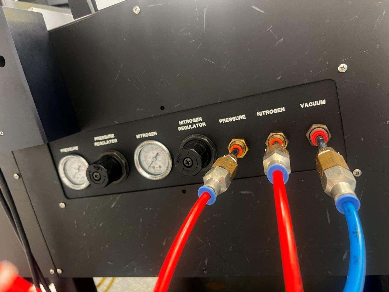
OAI J500 is a mask aligner for semiconductor lithography used in manufacturing of integrated circuits. The mask aligner is able to align a mask, or photomask, to a wafer with an accuracy in the nanometer scale. This is done through projection alignment and assisted by angular adjustment and a scan microscope. The mask aligner consists of an optical projection system and contains four main components: a light source, projection optics, a mask stage, and a wafer stage. The light source can be selected from laser, LED and arc lamp, with different wavelength and power output range. The projection optics magnifies and projects the mask onto the wafer, and features a reticle, a scan lens, and a condenser lens. The reticle is used to adjust the size, shape, and angular orientation of the mask pattern while the scan lens is used to correct the focus of the mask layout. The condenser lens is used to form the image of the mask on the wafer. The mask stage is used to hold the photomask and can be moved in three dimensions, enabling the alignment of the mask and wafer. It has a low velocity inertial system with a closed loop servo system to provide XYZ positional accuracy. The mask stage also houses the chromatic alignment optics which enables 3D compensation for aberrations induced by the projection optics. The wafer stage functions as the substrate for the alignment of the mask layer. It is made of ceramic material, and is capable of rotational alignment and ultra-smooth scanning with minimal stray fields. The alignment of the mask and the wafer requires a high degree of accuracy, with an optimal accuracy of 0.4 micrometers for patterning. J500 mask aligner is an important tool for semiconductor lithography used in the fabrication process of integrated circuits and other microelectronic components. It can provide nanometer level of precision and accuracy while maintaining high throughput and reliability in the most demanding semiconductor processes.
There are no reviews yet