Used ACTIVE ACT-560RMS-FA #293691017 for sale
URL successfully copied!
Tap to zoom
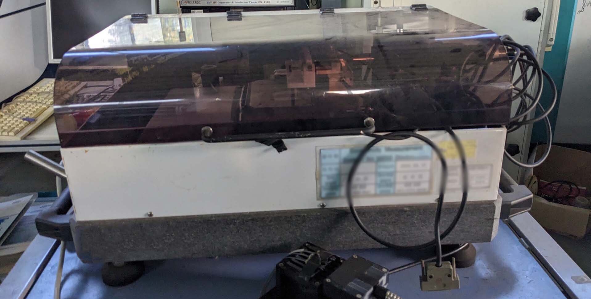

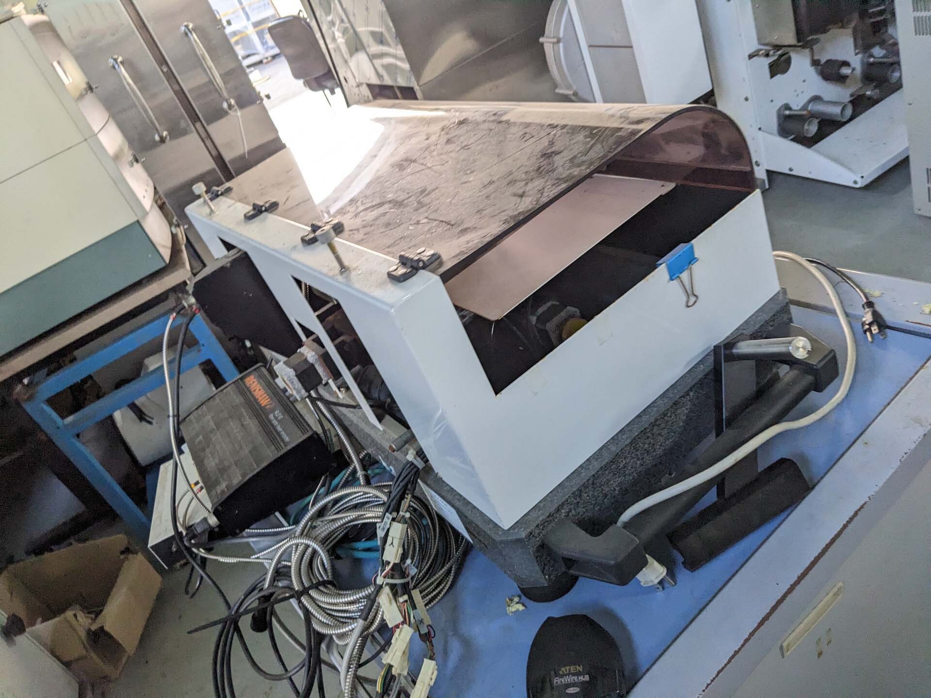
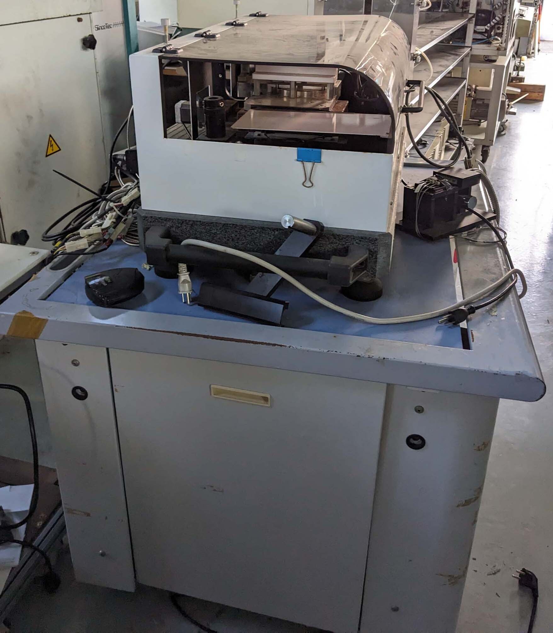
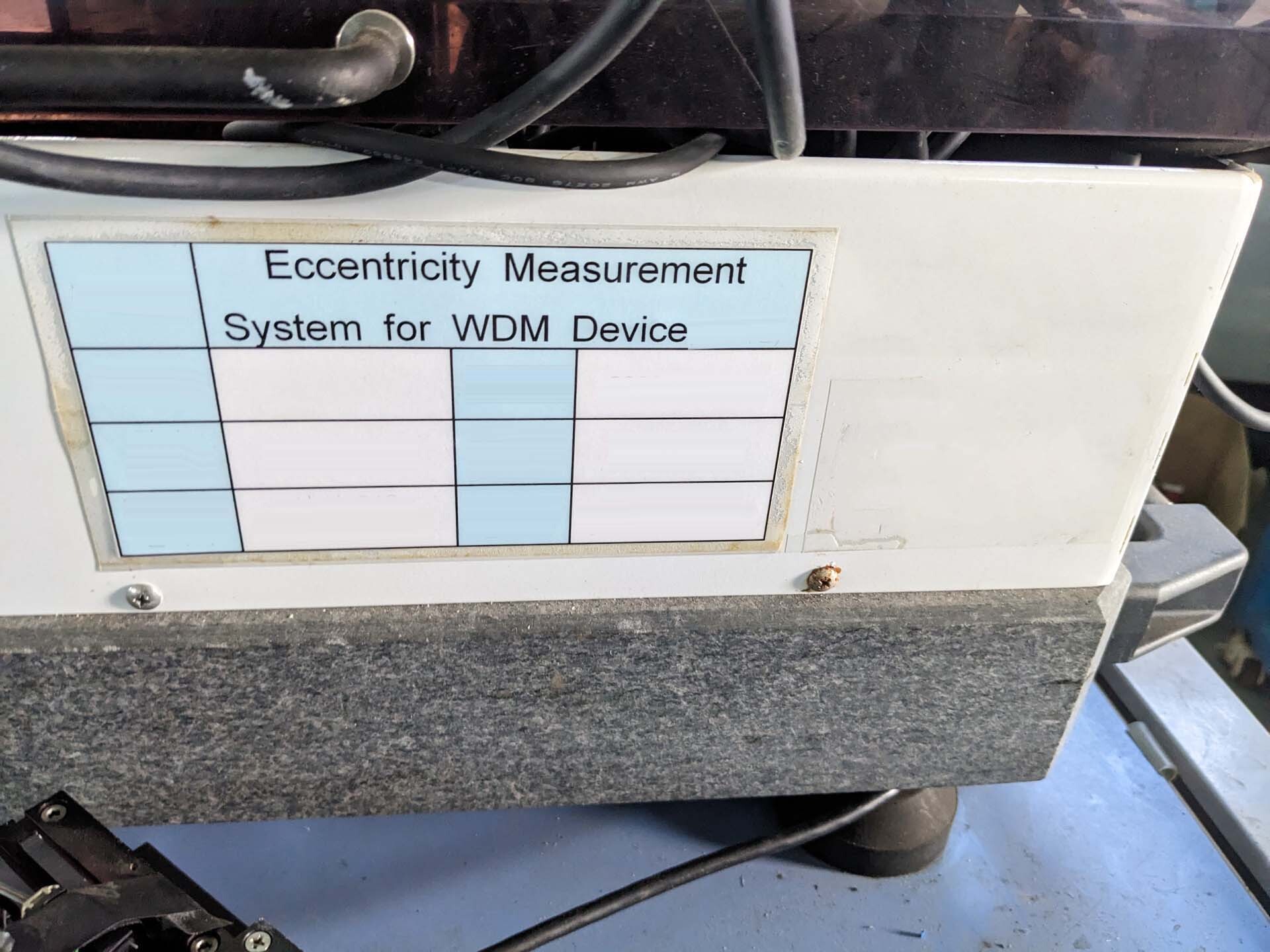
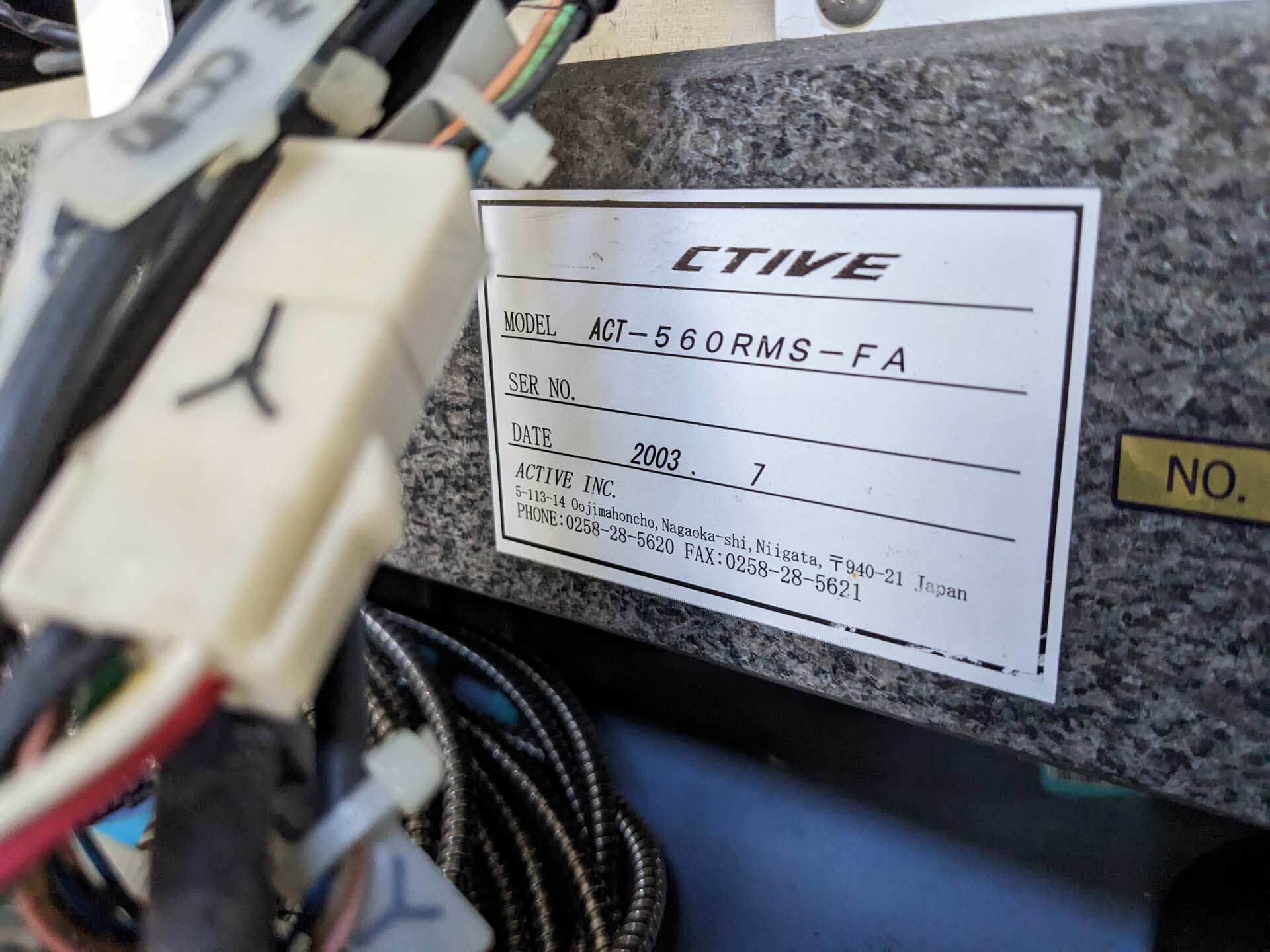
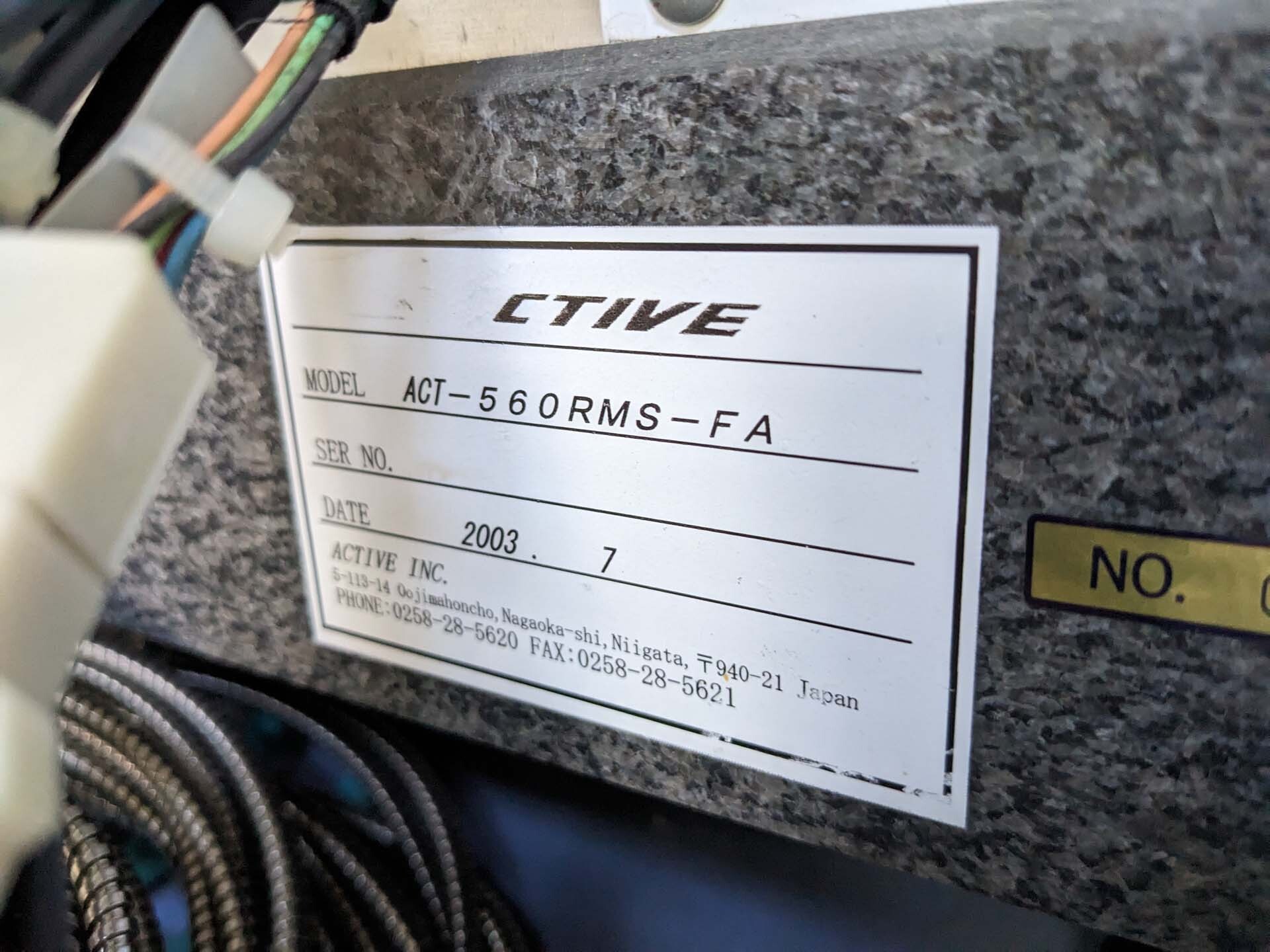
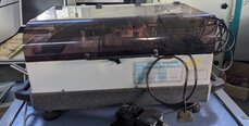
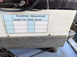
ACTIVE ACT-560RMS-FA is a cutting-edge mask and wafer inspection equipment designed to meet the demanding requirements of semiconductor manufacturing processes. This system incorporates advanced technologies to ensure high precision and accuracy in detecting defects and imperfections on masks and wafers, essential components in the production of integrated circuits. The heart of ACT-560RMS-FA unit lies in its sophisticated inspection capabilities, which are powered by a combination of optical and image processing techniques. The machine utilizes high-resolution imaging sensors and advanced algorithms to scan the surfaces of masks and wafers with unmatched precision. By capturing detailed images of the surfaces, the tool can identify even the smallest defects, such as particles, scratches, and contamination, that could compromise the quality and performance of the final semiconductor devices. For accurate defect detection, ACTIVE ACT-560RMS-FA employs a variety of illumination techniques, including bright-field and dark-field illumination. These techniques enable the asset to highlight different types of defects and improve the contrast between the defects and the background, making them easier to detect and analyze. In addition, the model offers automated focus adjustment and image enhancement features to further improve the quality and clarity of the captured images. ACT-560RMS-FA is equipped with a powerful image processing engine that leverages machine learning and artificial intelligence algorithms to categorize and prioritize defects based on their size, shape, and location. This intelligent defect classification equipment enables operators to quickly identify critical defects that require immediate attention, helping to streamline the inspection process and improve overall manufacturing efficiency. In addition to defect detection, ACTIVE ACT-560RMS-FA system also offers comprehensive metrology capabilities for measuring critical dimensions and overlay accuracy on masks and wafers. By leveraging advanced image analysis algorithms, the unit can accurately measure features such as linewidths, patterns, and alignment markers with submicron precision, ensuring that the semiconductor devices meet the required specifications and performance standards. One of the key advantages of ACT-560RMS-FA machine is its versatility and scalability, allowing semiconductor manufacturers to adapt the tool to their specific production requirements. The asset supports multiple inspection modes, including inspection of photomasks, reticles, and wafers at various stages of the manufacturing process. Furthermore, the model can be integrated seamlessly into existing production lines and automated workflows, enabling real-time monitoring and control of the inspection process. Overall, ACTIVE ACT-560RMS-FA represents a state-of-the-art solution for mask and wafer inspection in semiconductor manufacturing. With its advanced imaging technology, intelligent defect classification equipment, and comprehensive metrology capabilities, the system offers unparalleled accuracy and efficiency in detecting defects and ensuring the quality of semiconductor devices. By investing in ACT-560RMS-FA unit, semiconductor manufacturers can enhance their production processes, minimize defects, and improve the yield and reliability of their semiconductor products.
There are no reviews yet