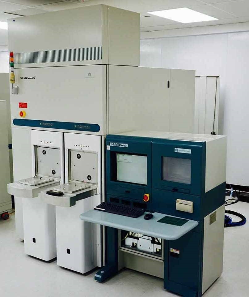
Used AMAT / APPLIED MATERIALS SemVision G2 Plus #9280524 for sale
It looks like this item has already been sold. Check similar products below or contact us and our experienced team will find it for you.
Tap to zoom


Sold
ID: 9280524
Wafer Size: 12"
Vintage: 2002
Defect review system, 12"
Wafer handling:
Loader: AMAT ADO with RFID
ETU, 12"
ITU, 12"
FFU with ULPA Filter
SEM Column G2
EDX Column
Column tilts: 45 Deg
Wafer rotation option
Stage wafer holder: 3 PIN
Aligner optical microscope 5x, 20x, 100x
Pal (On the OTW, cassette / Slot 1: Delta X= 500 μm, Delta Y= 500 μm
ITU Repeatability: Delta X and Delta Y < 20 μm
Stage accuracy: Delta X and Delta Y < 1.5 μm
MTR:
Delta X: 50
Delta Y: 30 μm
Resolution at 1 KeV: 3 nm
Focus map / focus offset: 90% defect with Delta Z < 3 μms
Automatic defect offset / XY Map: 95% defects with Delta X < 1.5 μm and Delta Y < 1.5 μm
EDX resolution: 4 nm
Wafer throughput: 12 Wafers / Hours
Defects throughput >1000 Defects / Hour
Cleanliness front side: 0.013 PWP / cm² > size at 0.2 μm
Largest load ampere rating: 8 A
Full load current: 10 A
Interrupt current: 10,000 Amps
Power requirements:
1-120 VAC, Single Phase, 3 Wire
208 V, 3 Phase, 5 Wire, 50/60 Hz
2002 vintage.
AMAT/AMAT / APPLIED MATERIALS SemVision G2 Plus mask & wafer inspection equipment is an advanced, automated optical inspection (AOI) system designed for semiconductor and display device manufacturers. The unit consists of a dual-laser wafer scanner, advanced image capture and pattern recognition algorithms, and digital feature measurement capabilities. AMAT SemVision G2 Plus machine offers superior performance for automatic photomask defect detection, mask layout verification, and wafer-level defect review, allowing faster process speeds with improved accuracy. The G2 Plus mask & wafer inspection tool features two high-power laser sources to create a bright, uniform, evenly distributed light source. The dual-laser technology offers improved performance over single-laser systems and ensures quick and accurate imaging of the mask surface with fewer false defect detections. Advanced imaging technology captures full and partial pattern information with pixel-level resolution, providing superior edge detection and brightness balance, and increasing defect sensitivity across the entire mask area. APPLIED MATERIALS SemVision G2 Plus asset also features a wide range of advanced pattern recognition techniques, including Diffractive Optical Elements (DOEs) and defect detection using Coplanar Difference Imaging (CDI). A built-in library of inspection templates provide users with a standard model for testing similar masks and wafers, so inspection results are consistent and reproducible. The model can also be enhanced with the addition of customized optics, such as LED or continuous wave lasers, and higher power levels for improved defect analysis. SemVision G2 Plus equipment improves inspectability for a variety of device architectures, including flip chip, BGA, wafer-level chip scale, and fan-in/fan-out packaging. Its user-friendly interface allows for intuitive operation, with real-time defect detection and analysis via on-screen displays. With its optimized algorithms and advanced measurement capabilities, the G2 Plus system helps increase productivity and improve quality assurance for maximum yield.
There are no reviews yet