Used AMAT / APPLIED MATERIALS SemVision #293762276 for sale
URL successfully copied!

Tap to zoom
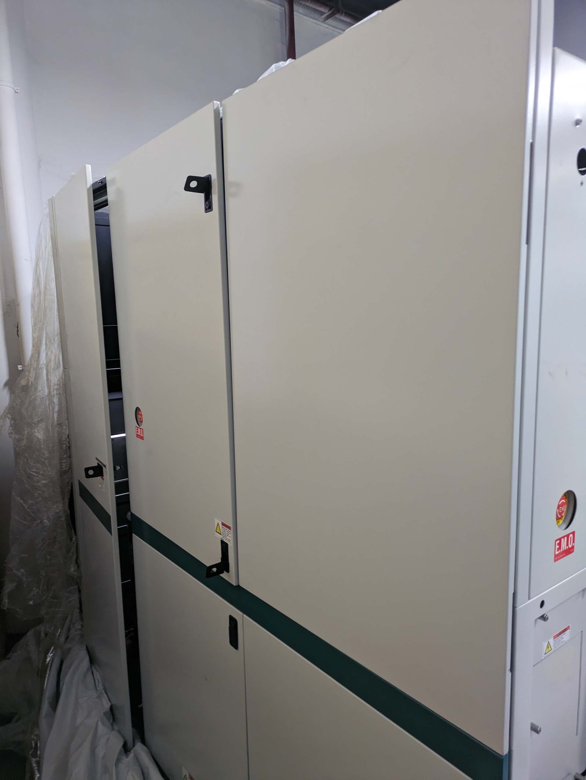

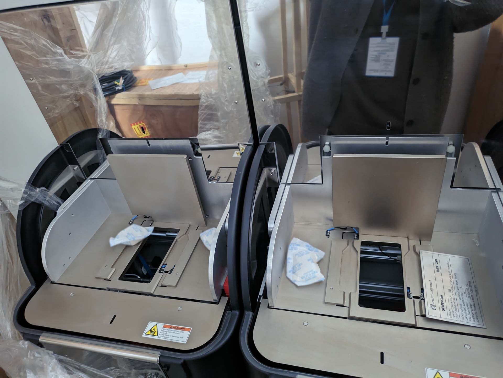
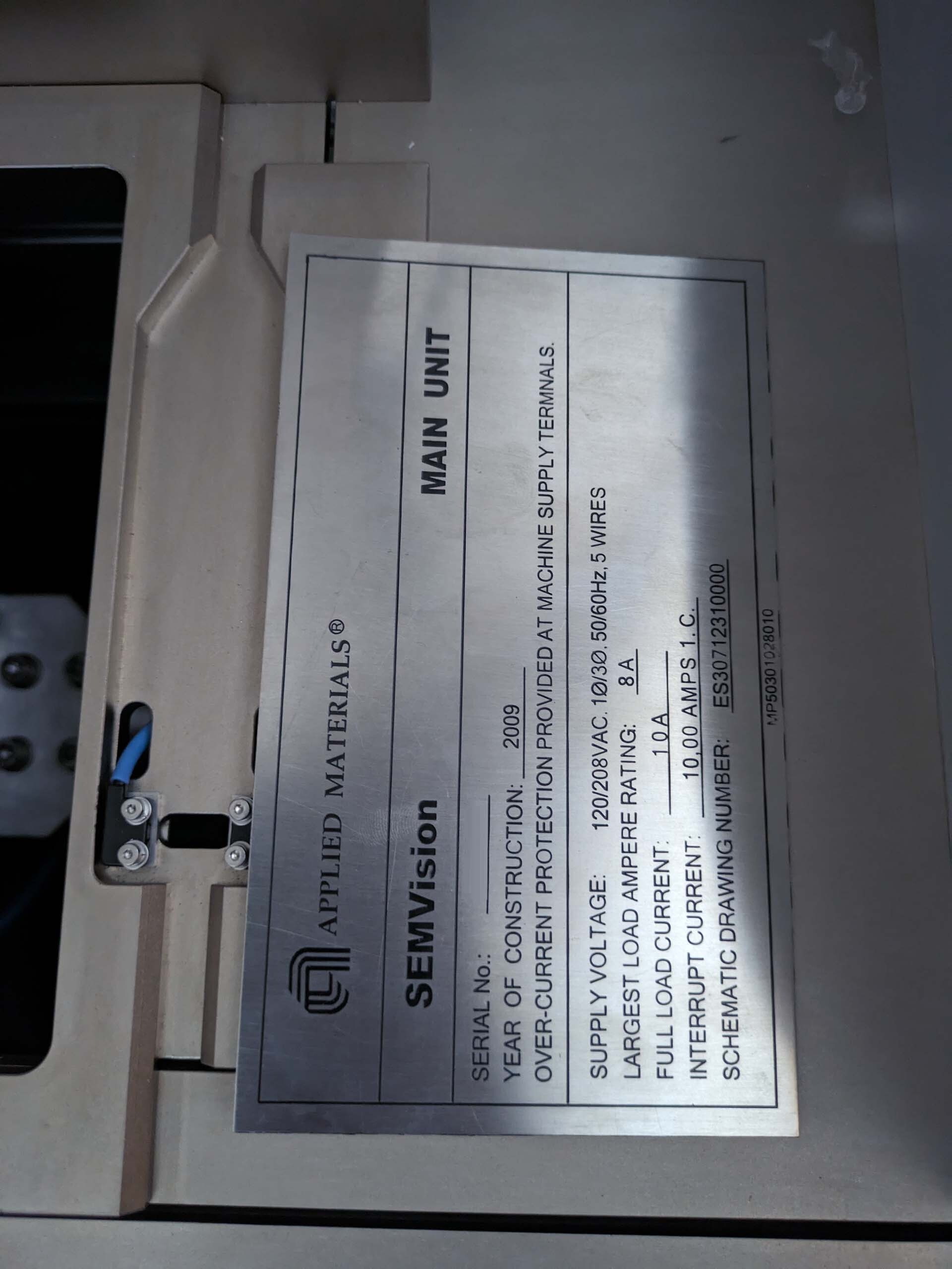
ID: 293762276
Wafer Size: 8"
Vintage: 2009
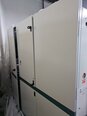
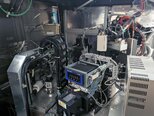
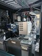
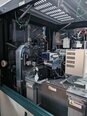
Defect review system, 8"
Controller
2009 vintage.
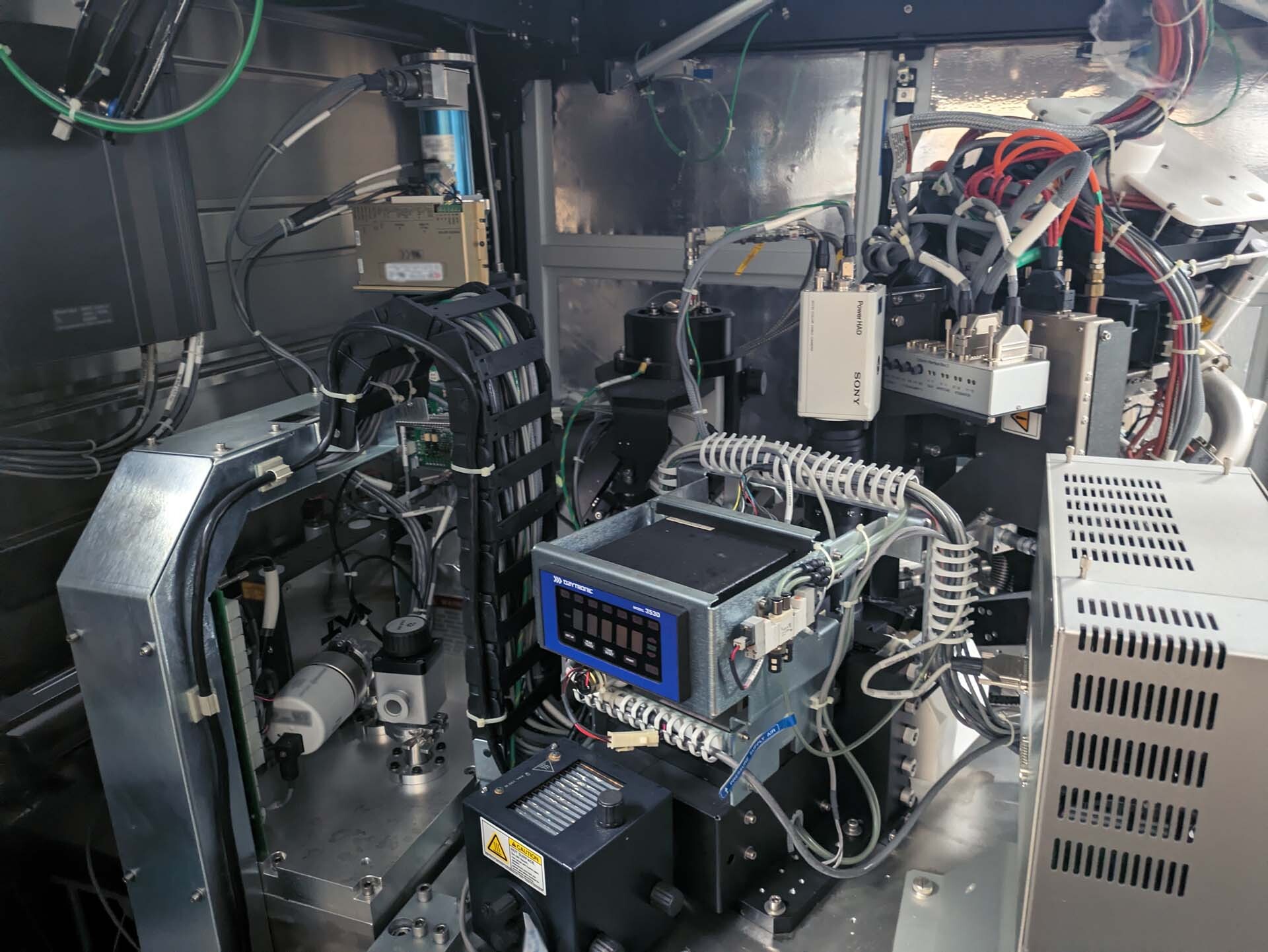
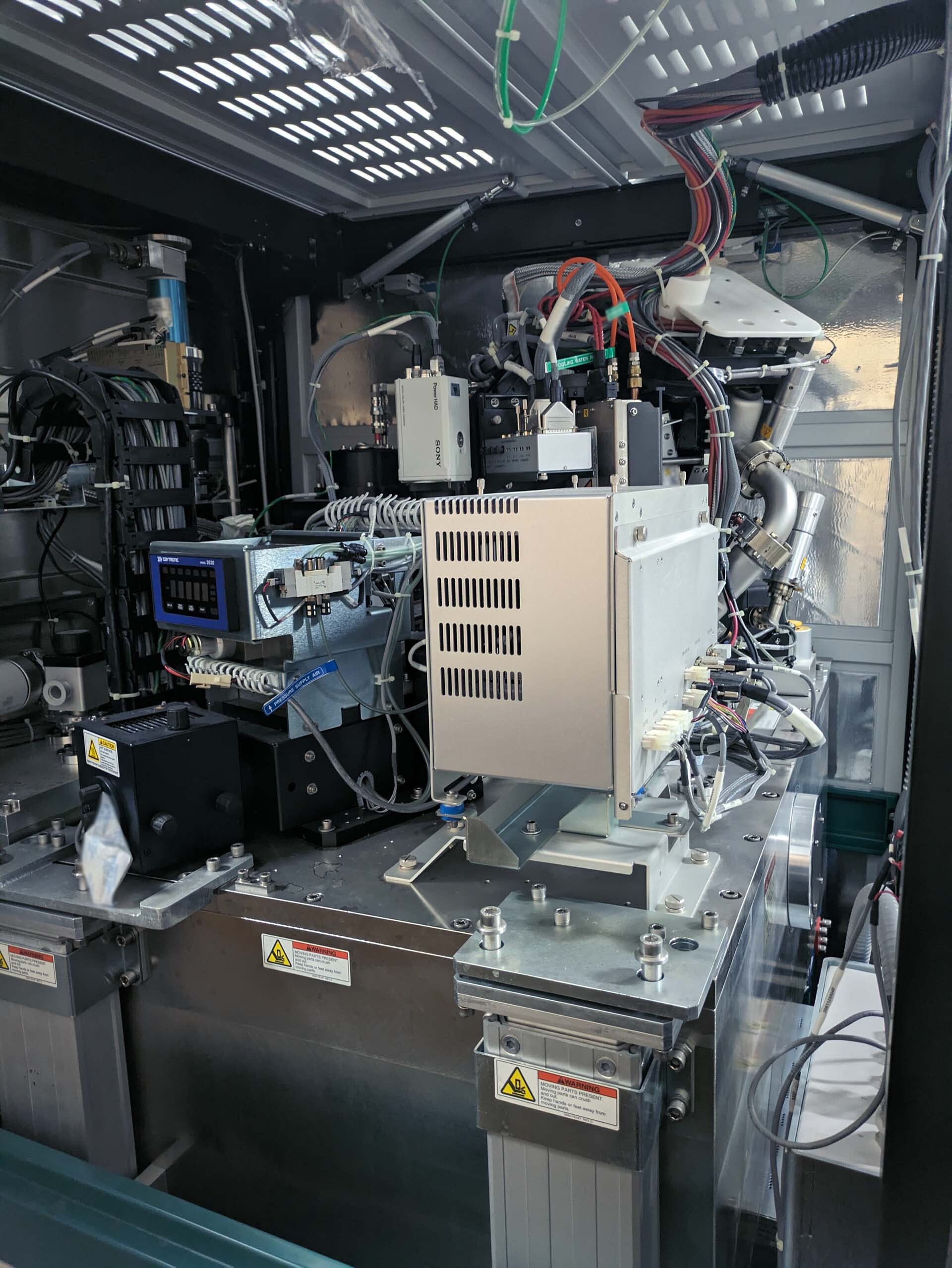
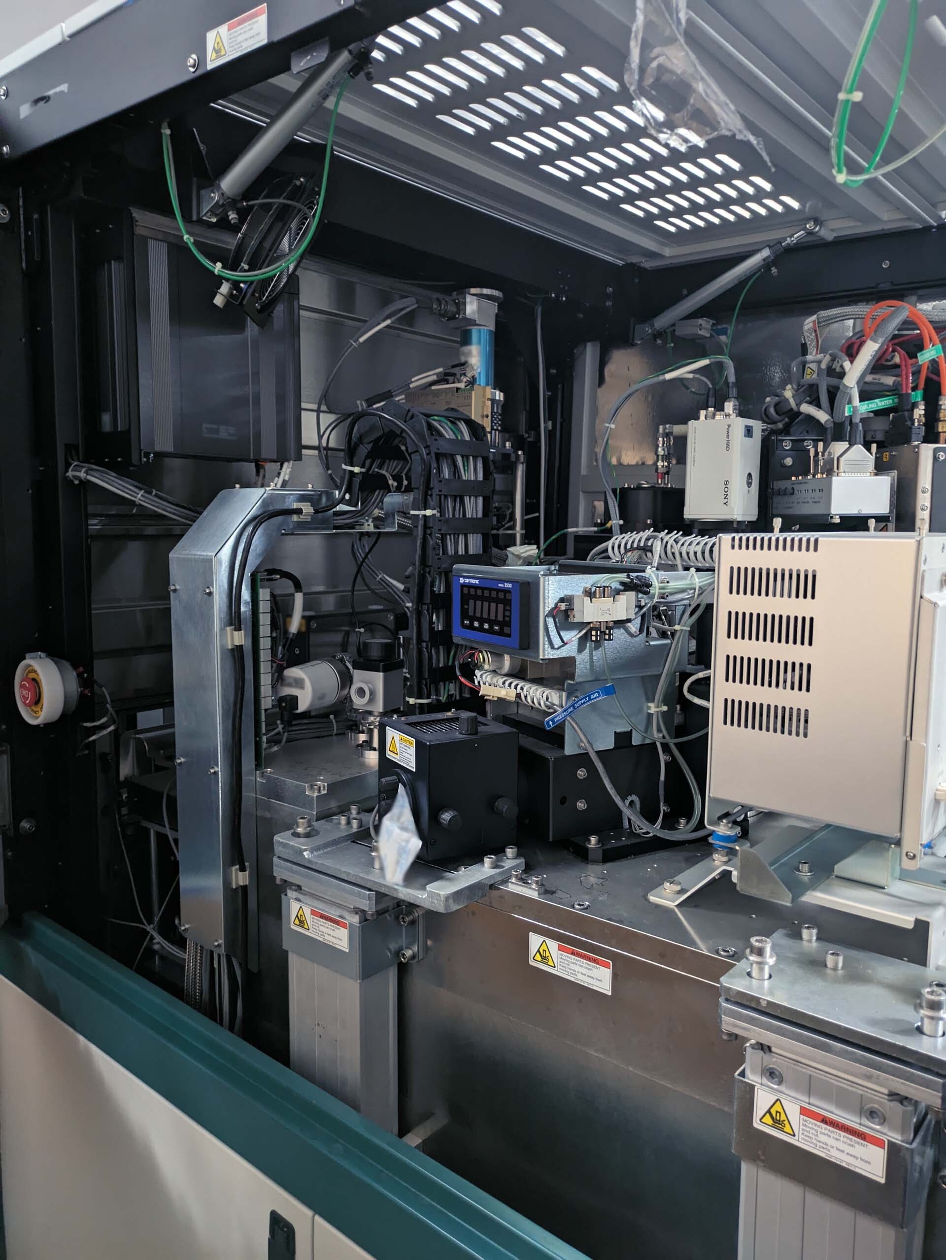
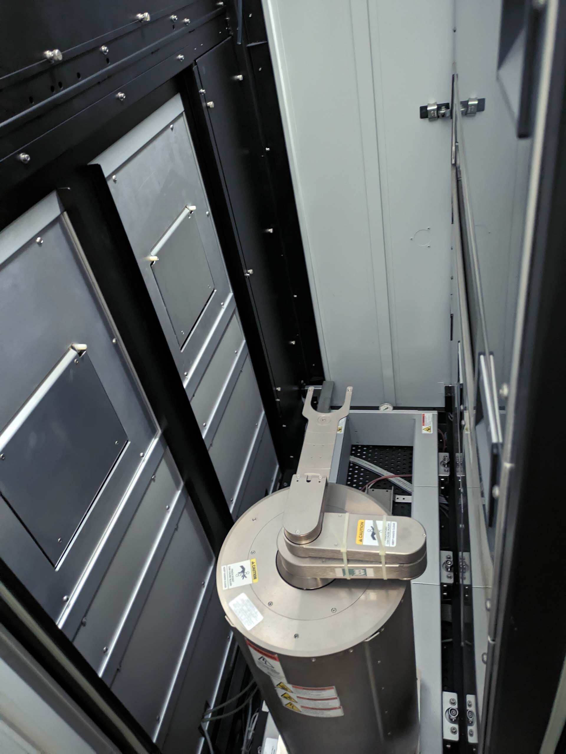
AMAT / APPLIED MATERIALS SemVision Mask & Wafer Inspection Equipment is an innovative and powerful imaging and inspection solution for photomask and wafer applications in the semiconductor industry. The system provides real-time, defect-free images of masks and wafers enabling advanced defect detection and 100% automated defect detection at the pixel level. This comprehensive unit features advanced illumination technology, a user-friendly interface, and a variety of image acquisition and analysis capabilities. The machine comes with a high-quality color camera which offer excellent image resolution, dynamic range, and noise characteristics, enabling a variety of imaging techniques for a wide range of feature sizes. A powerful, automated illumination tool provides illumination for various types of defects, and an advanced control board for integrated real-time control of the entire asset. The model also boasts an intuitive, graphical user interface for easy setup and control, and a variety of image analysis and visualization tools for defect detection and analysis. AMAT SemVision Equipment has proven to be an invaluable tool in the semiconductor world. It can detect defects of any size and in any layer, ensuring 100% inspection of masks and wafers with the highest sensitivity and accuracy. Advanced imaging capabilities allow the operator to quickly determine the type of defect, and the system includes a powerful defect classification module for automated defect ID and classification. This ensures the highest quality images and results in higher yields of good devices. The unit also features a host of automated image stitching and reconstruction algorithms, as well as auto characterization and mask handling technologies to ensure accurate measurement of structures in masks and non-flat surfaces. The integrated mask handling technology allows the machine to automatically handle, align and reject masks with up to 480,000 defects in less than 1 minute. APPLIED MATERIALS SemVision Mask & Wafer Inspection Tool is a powerful and reliable tool for semiconductor industries, providing accurate and reliable defect detection and analysis. Its user-friendly design and intuitive graphical interface ensures ease of operation, while advanced image analysis and defect classification capabilities provide a comprehensive solution for mask and wafer inspection applications. This asset is a must-have for any semiconductor manufacturer, providing the highest quality images and results for higher yields and better yields.
There are no reviews yet