Used AMAT / APPLIED MATERIALS SemVision #293767211 for sale
URL successfully copied!
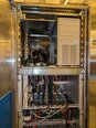
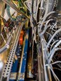
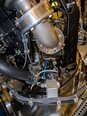
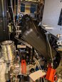

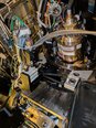
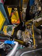
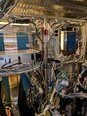
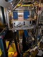
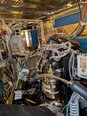
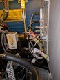
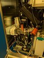
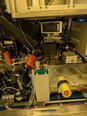
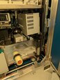
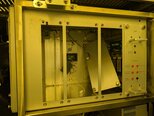
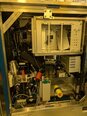
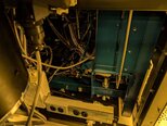
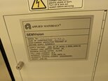
Tap to zoom
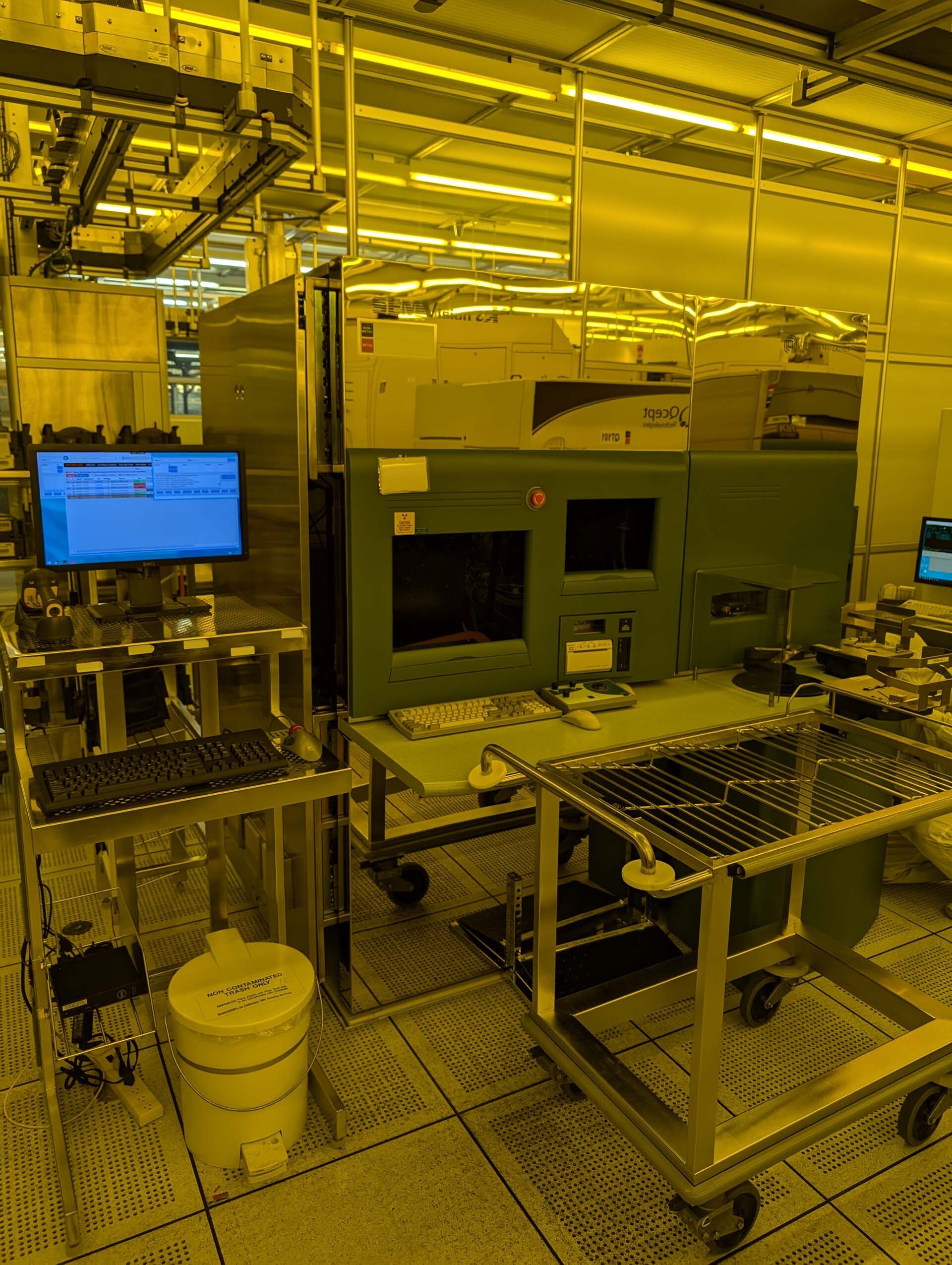

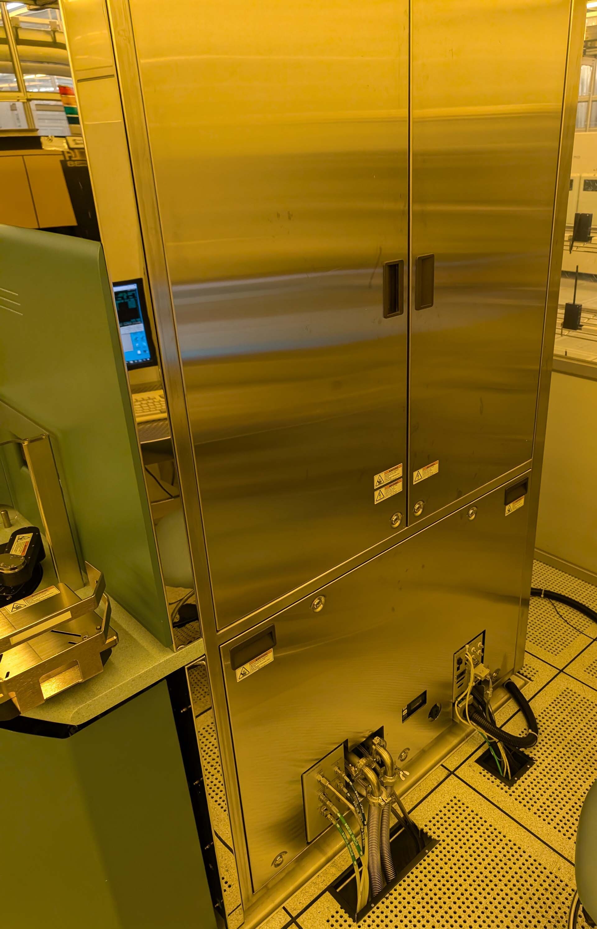
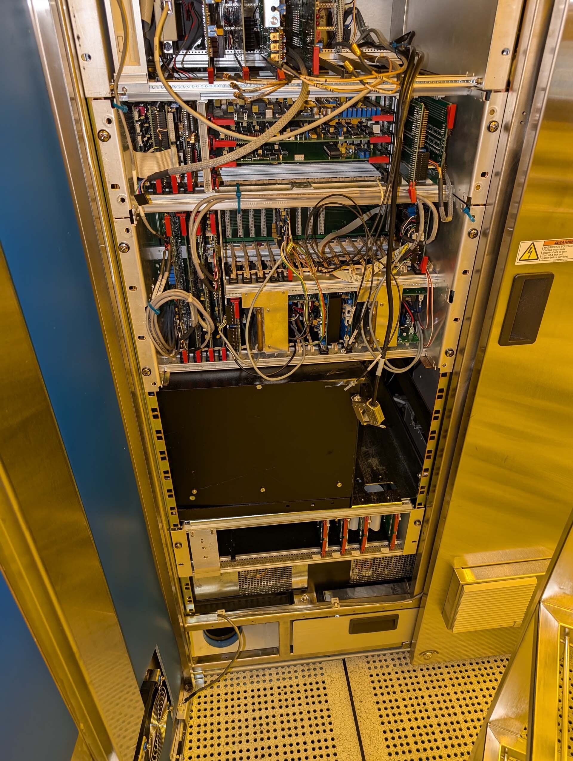
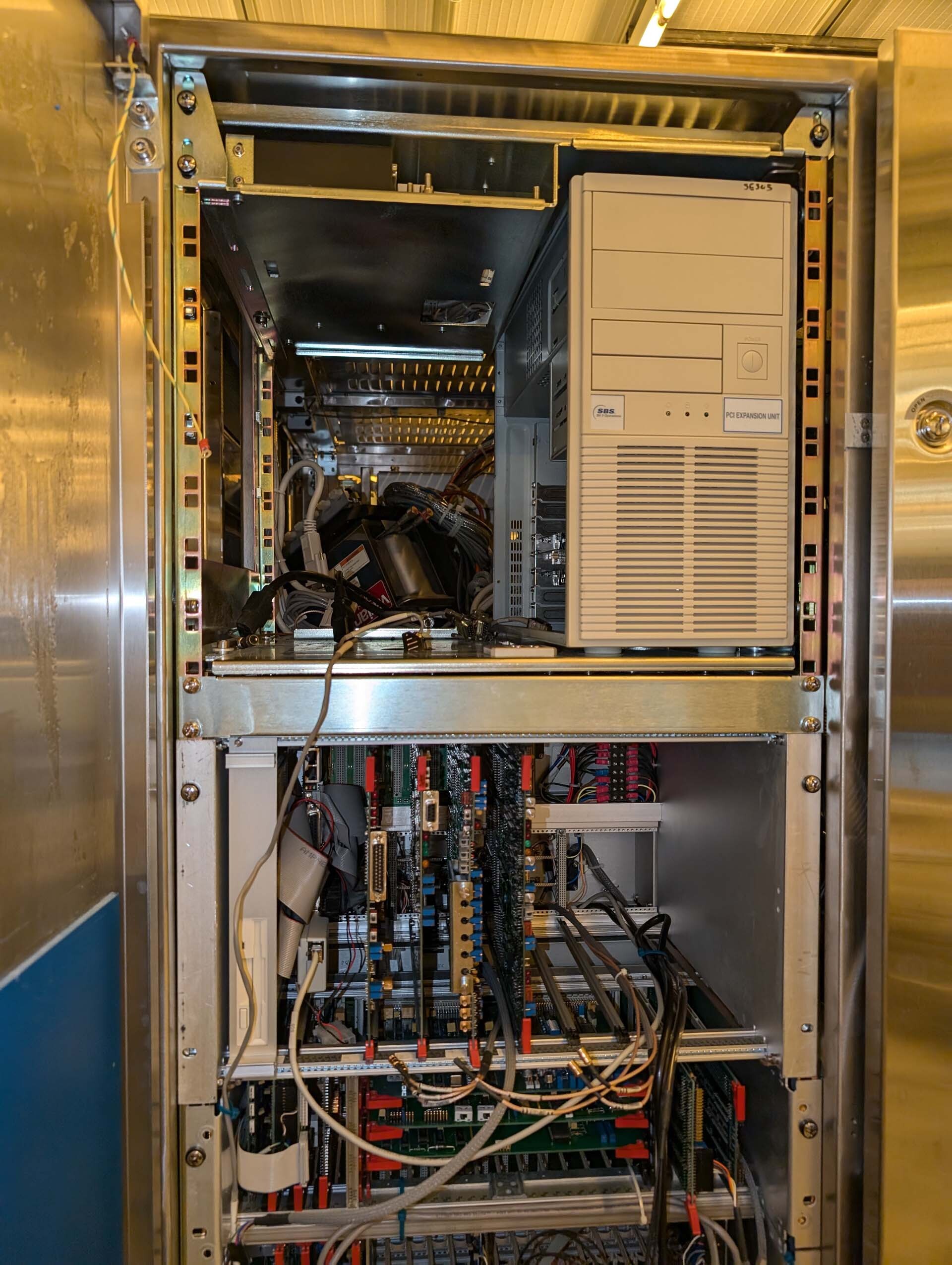
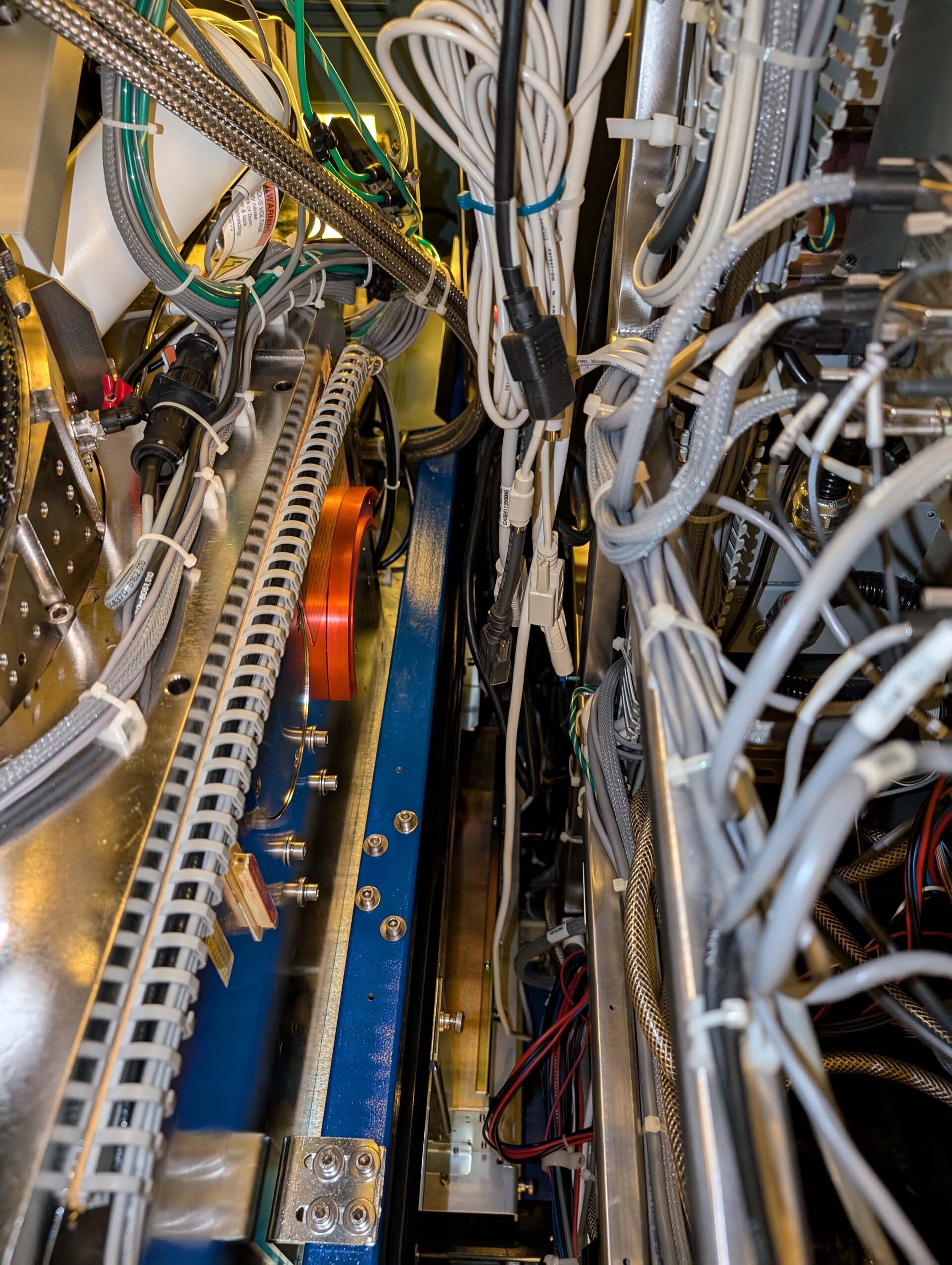
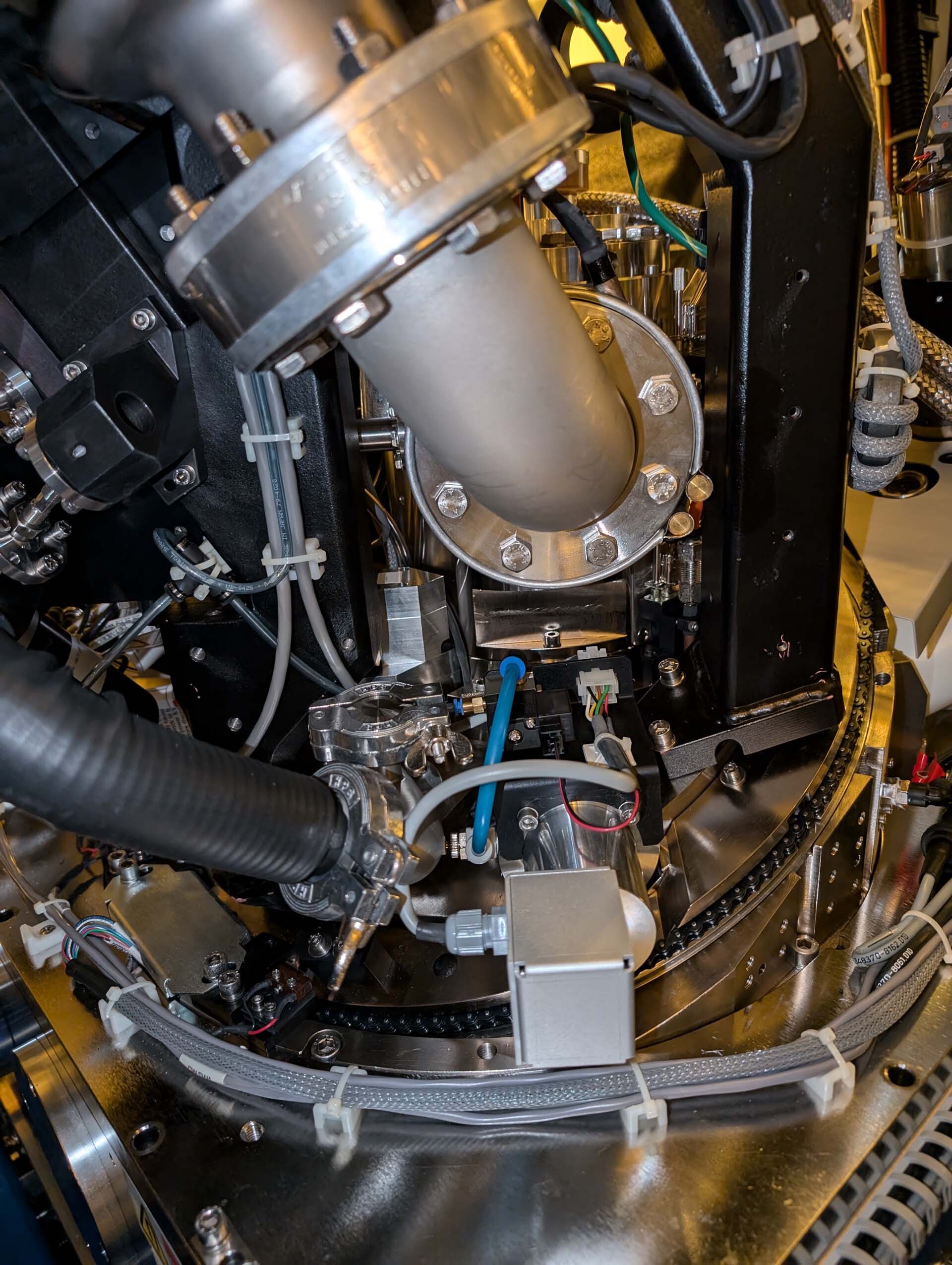
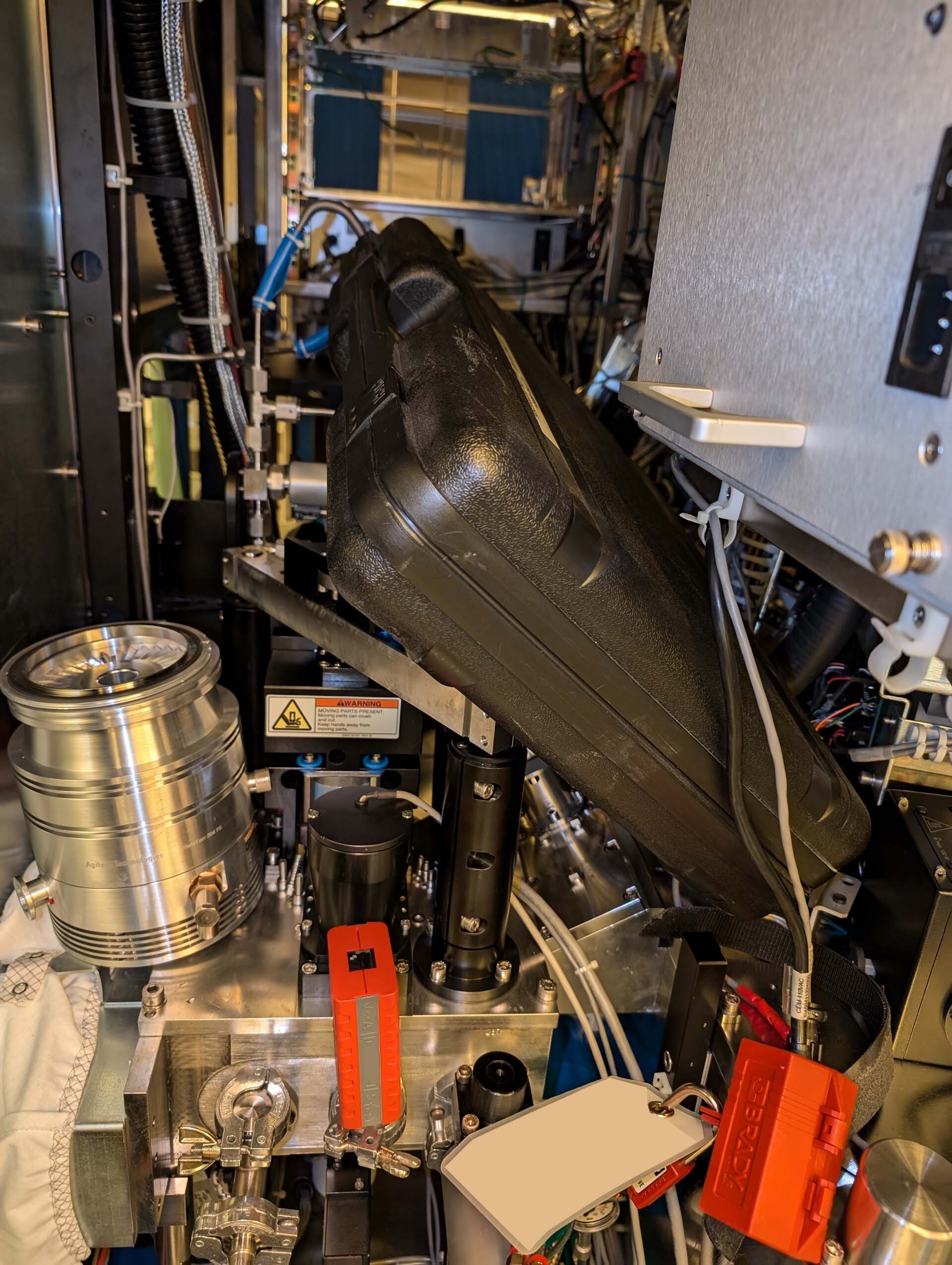
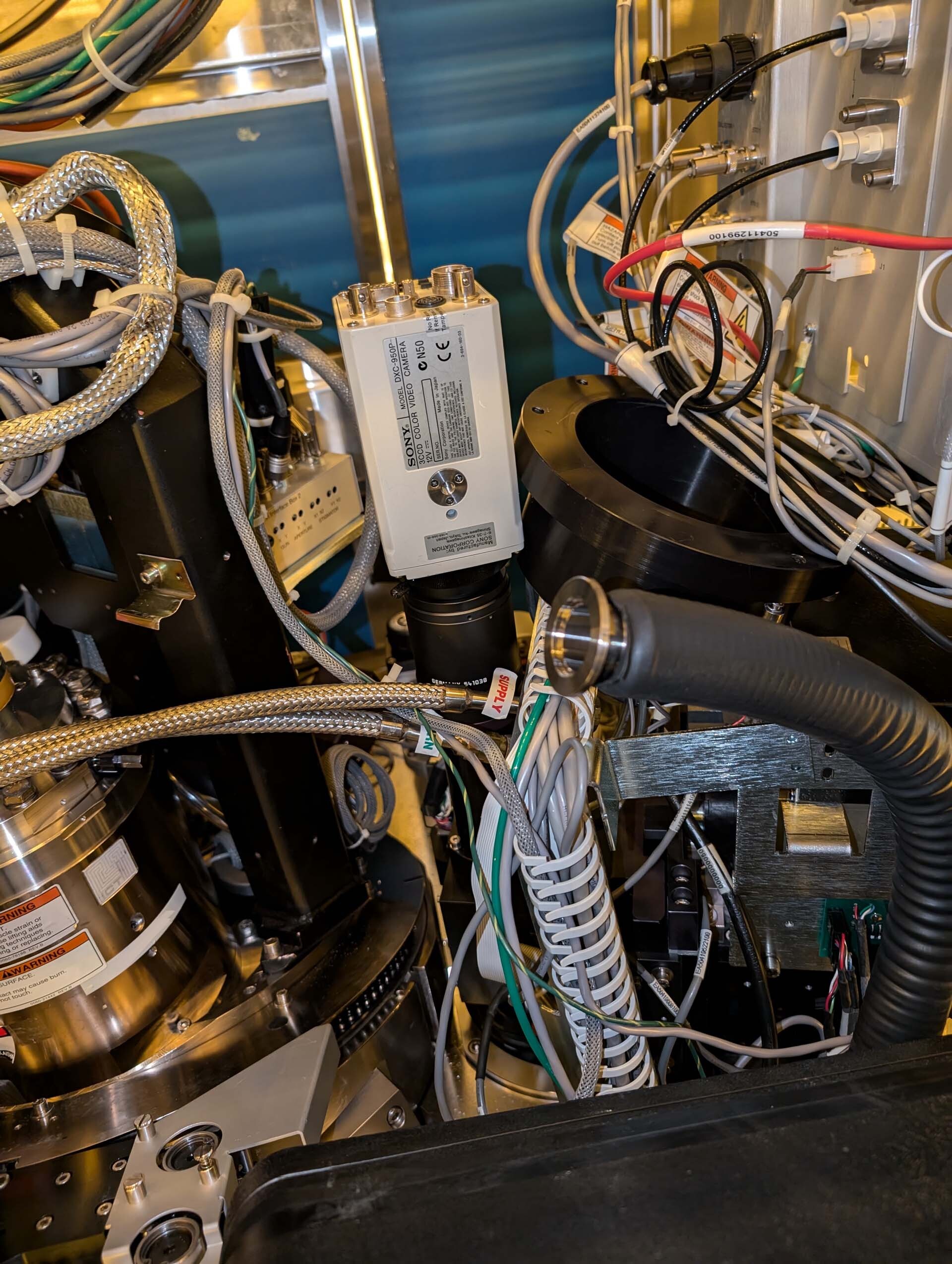
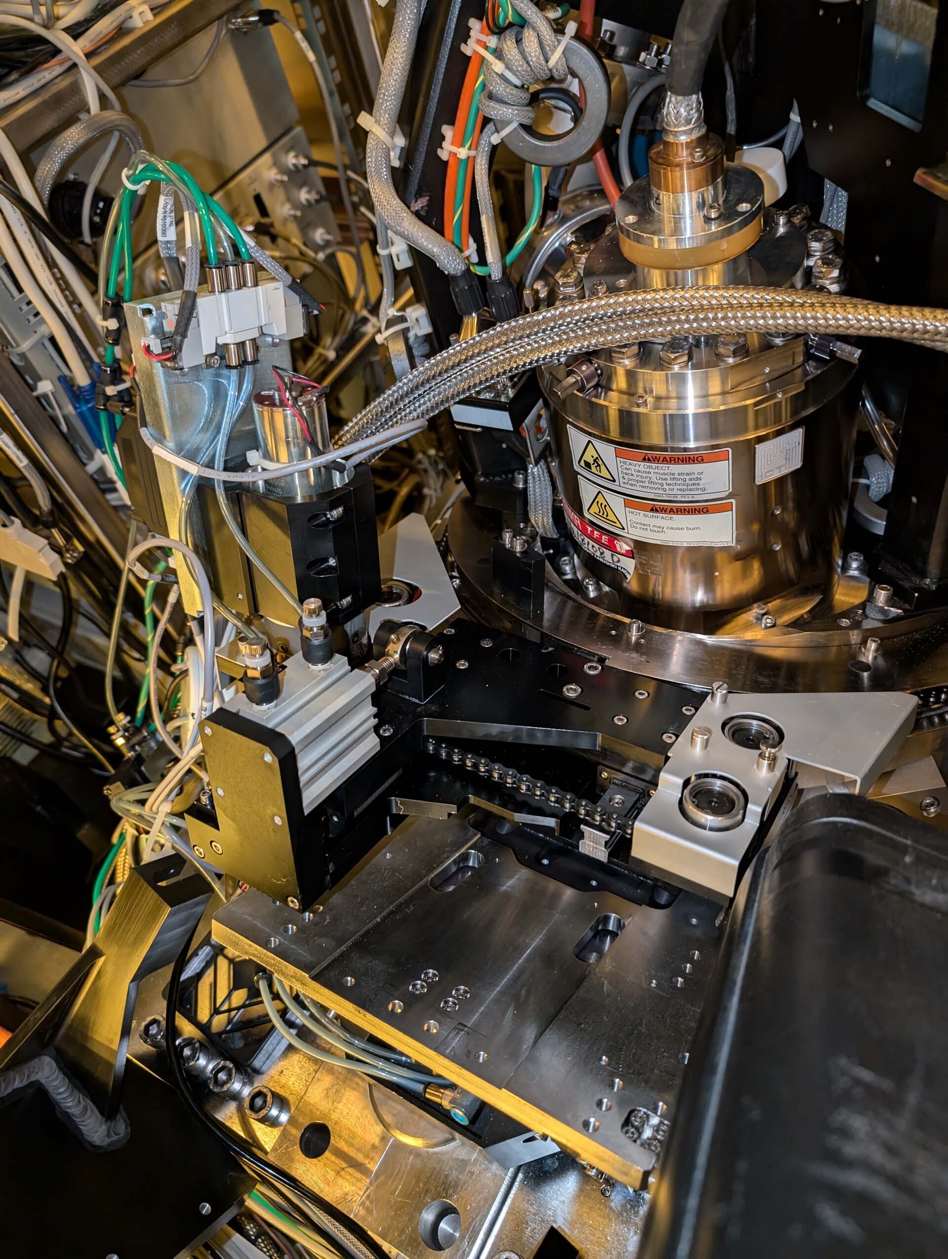
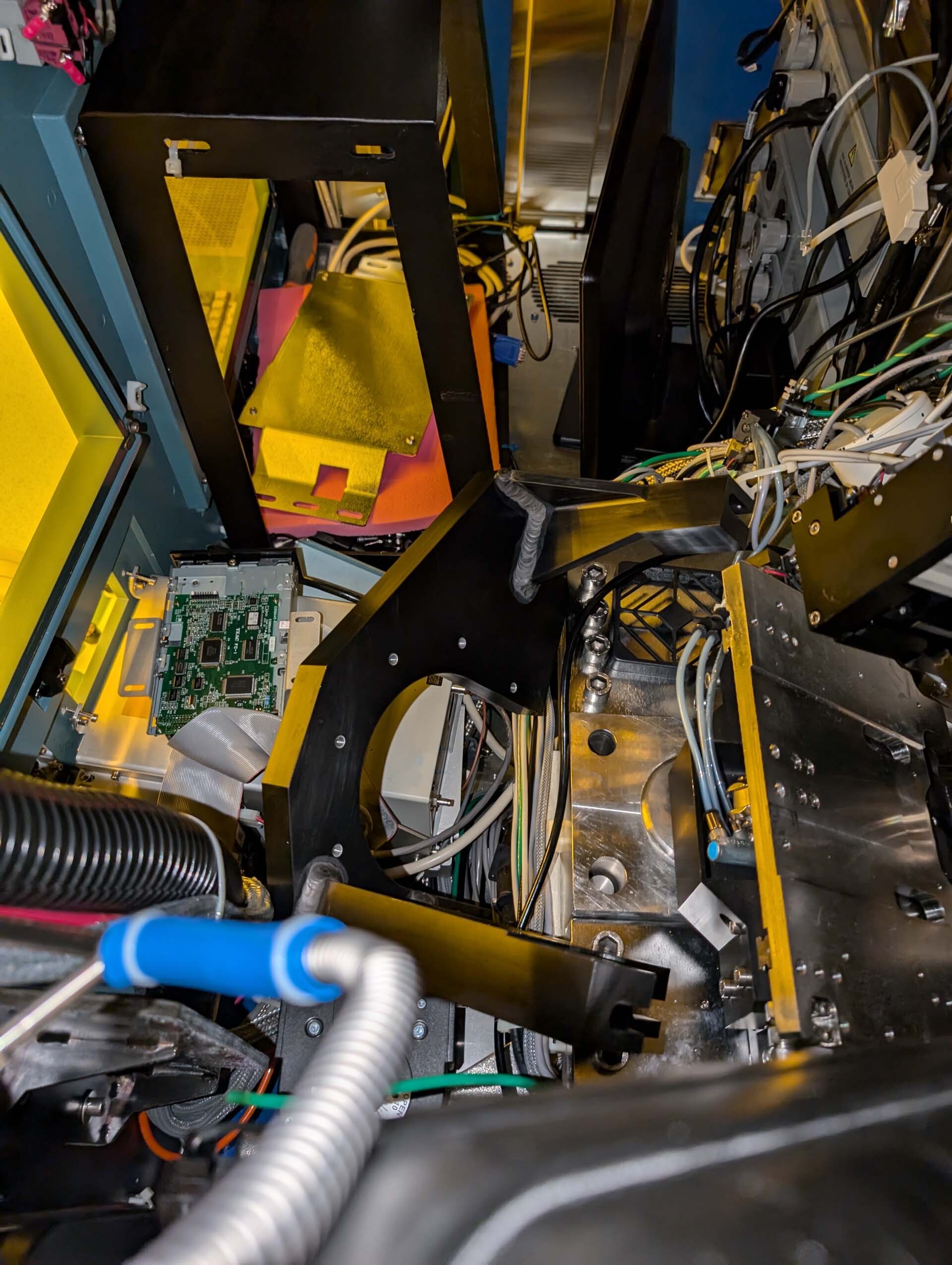
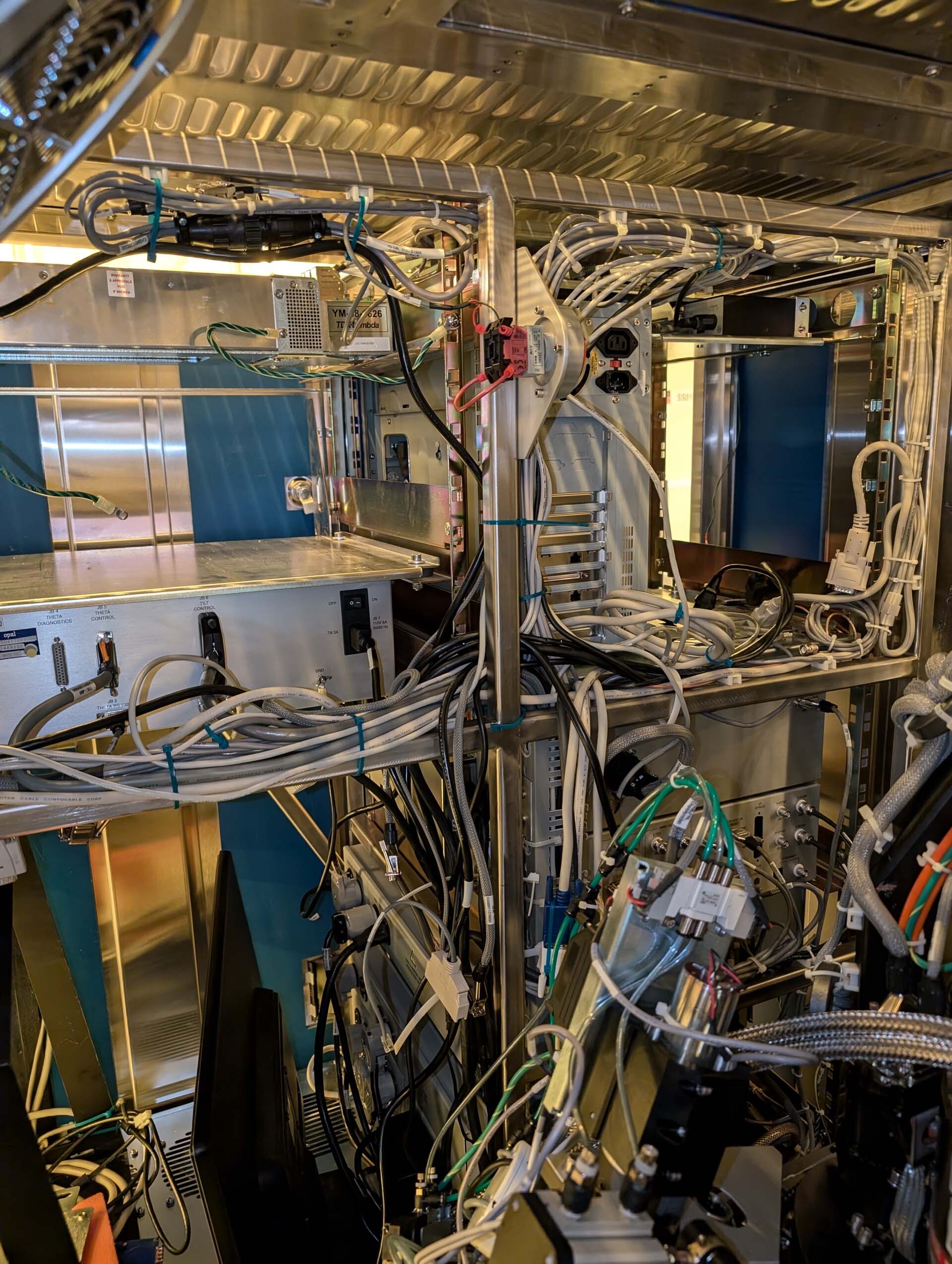
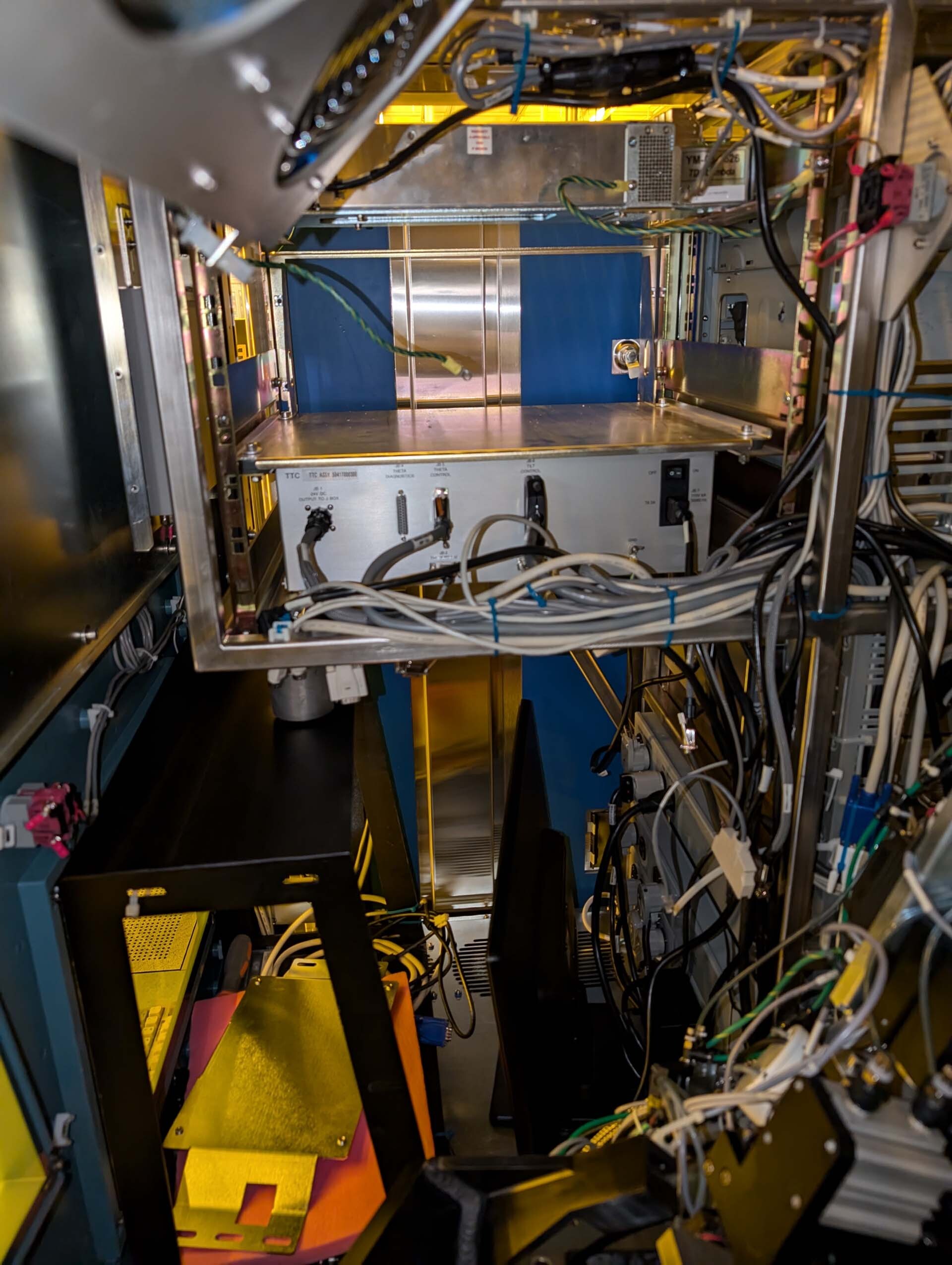
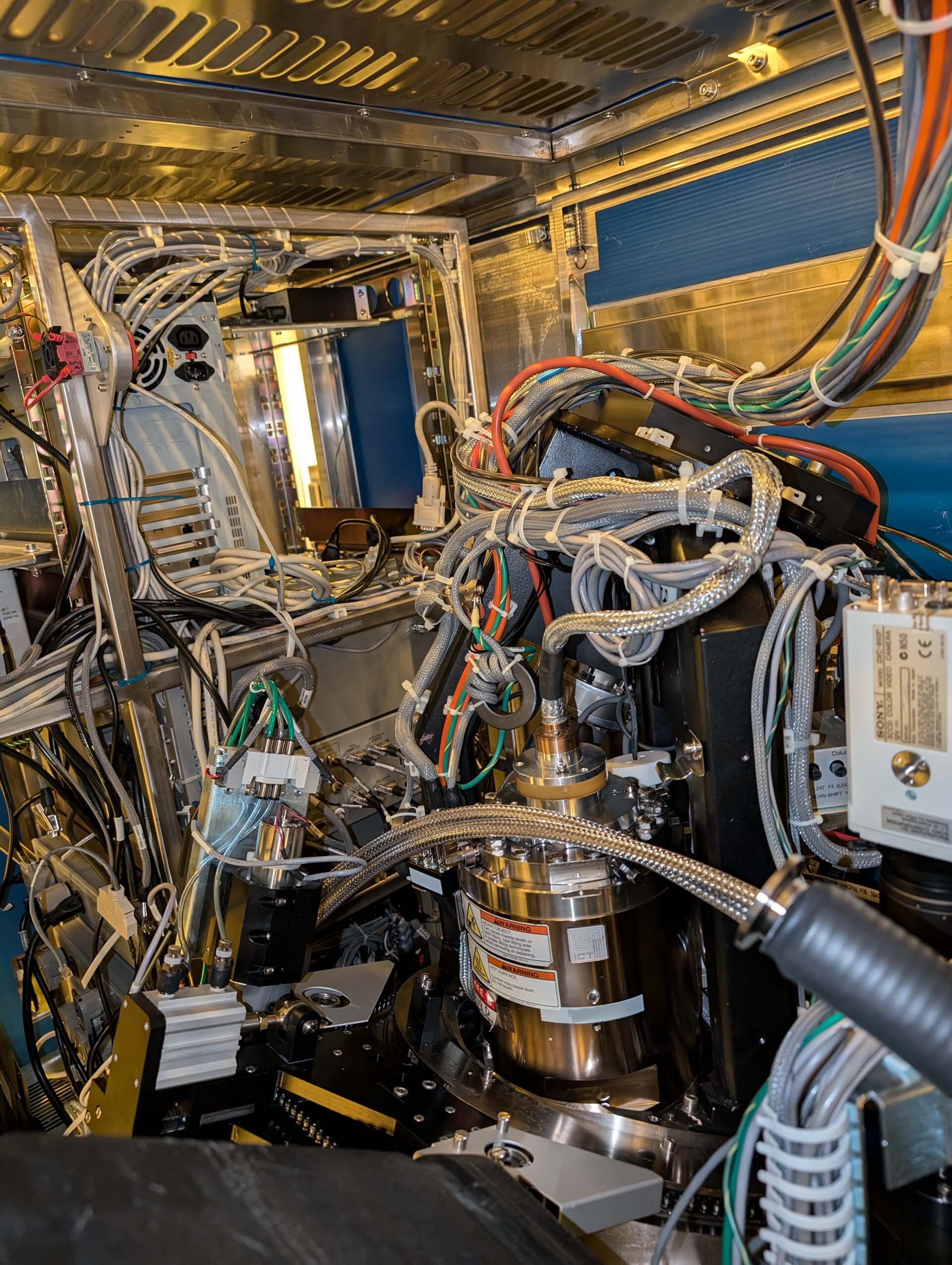
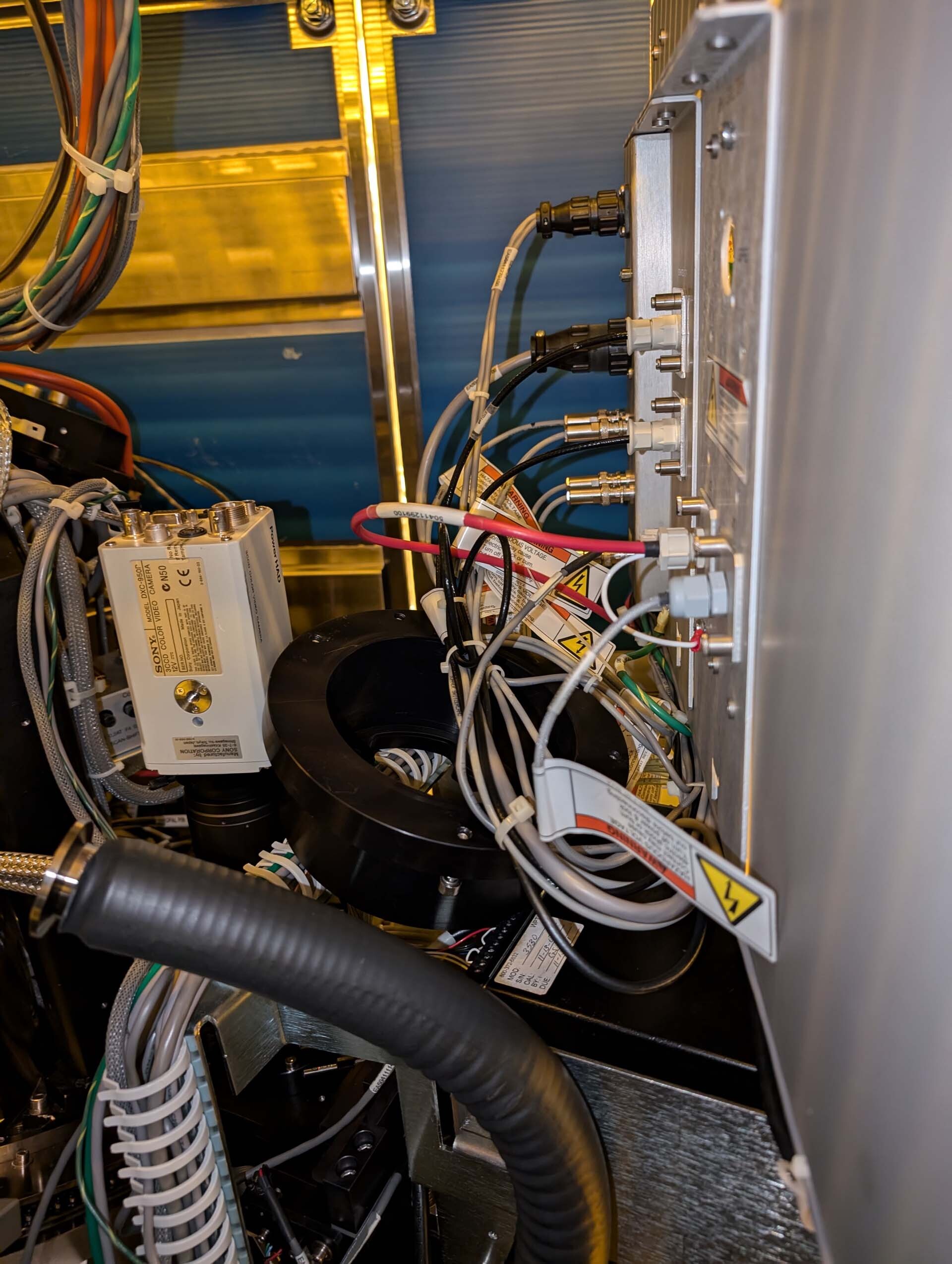
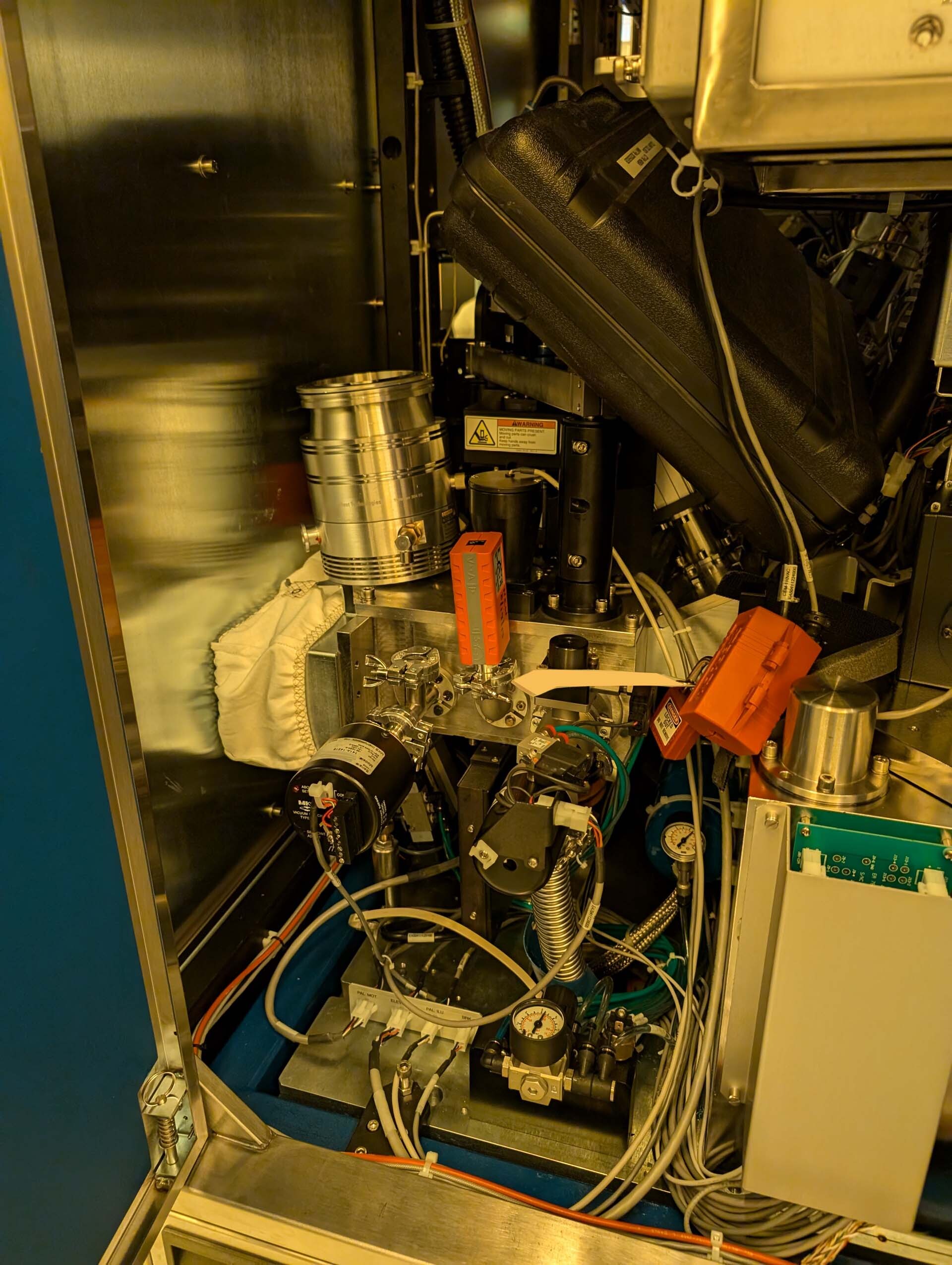
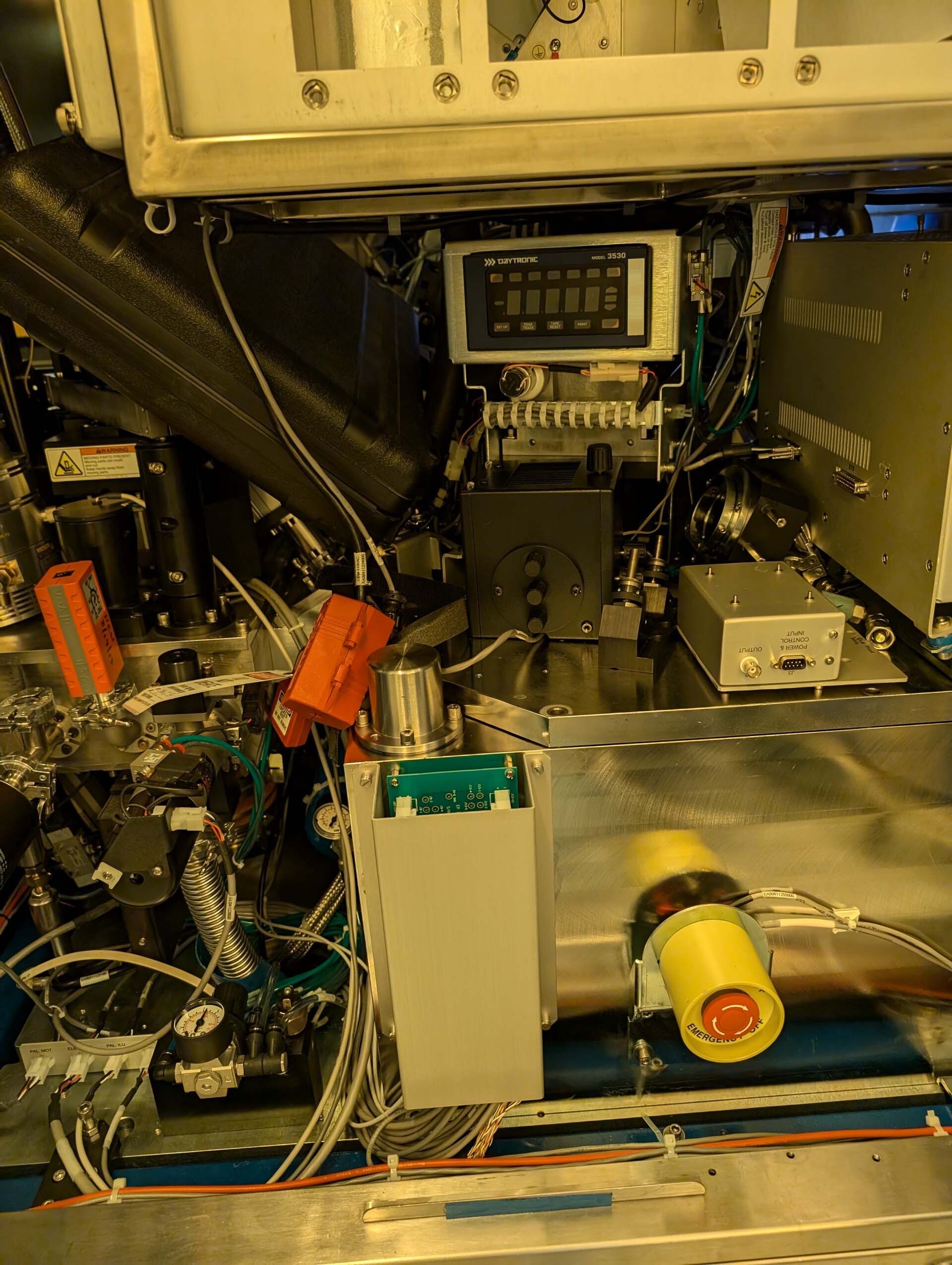
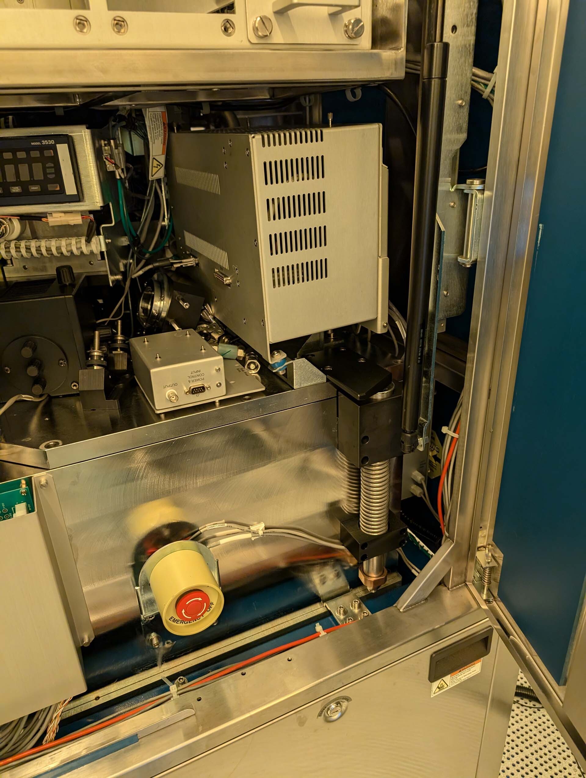
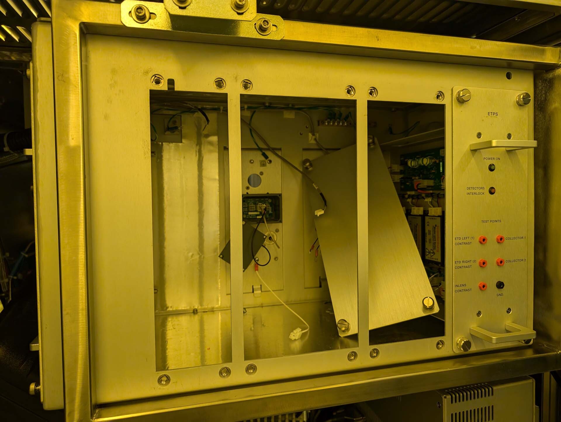
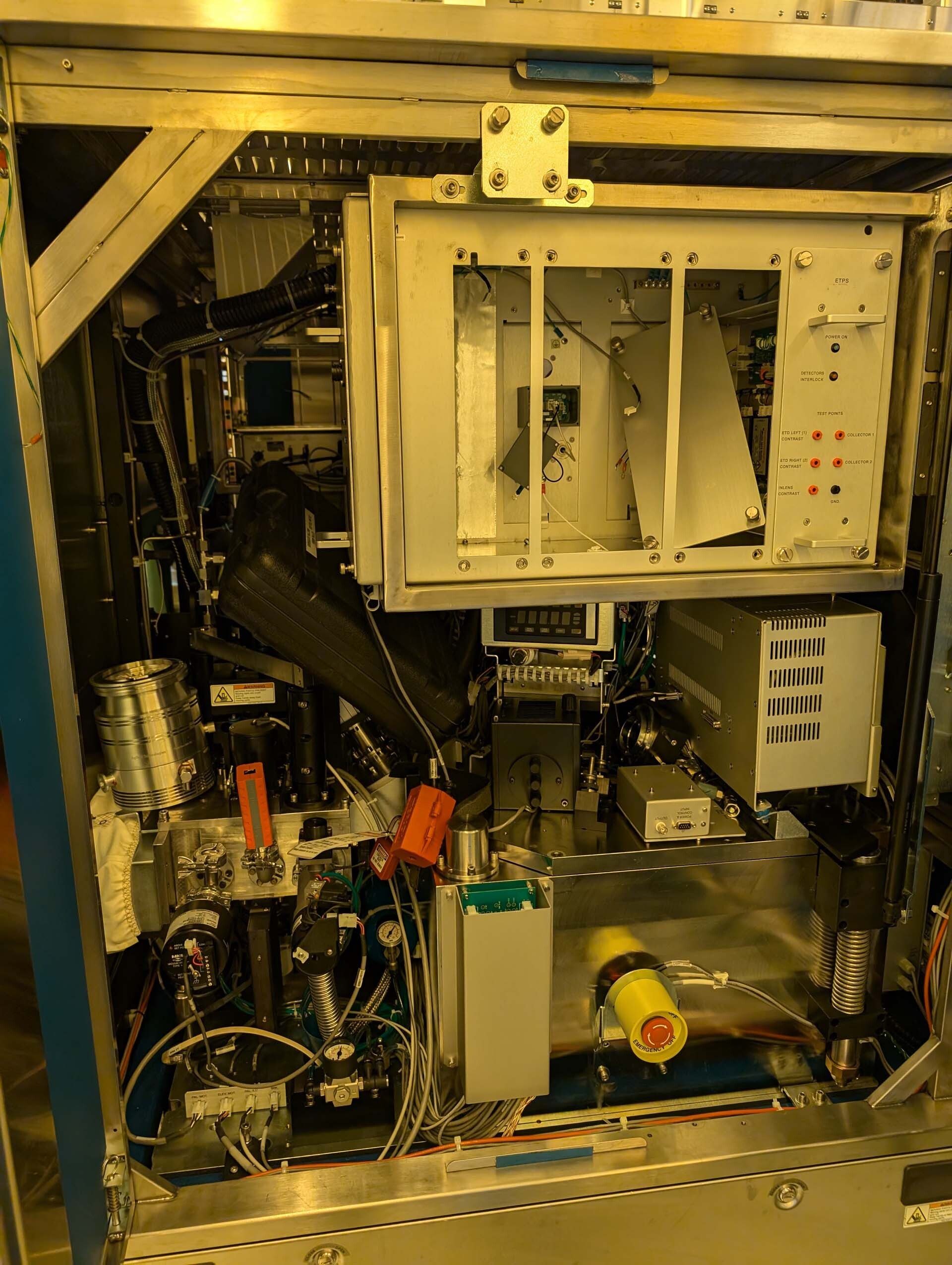
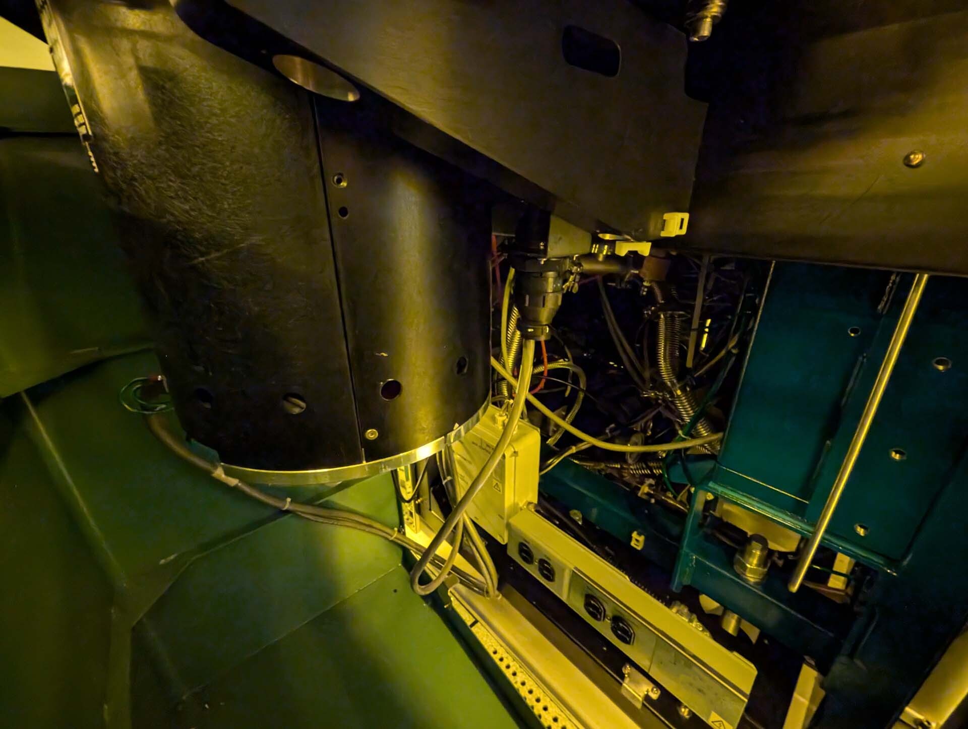
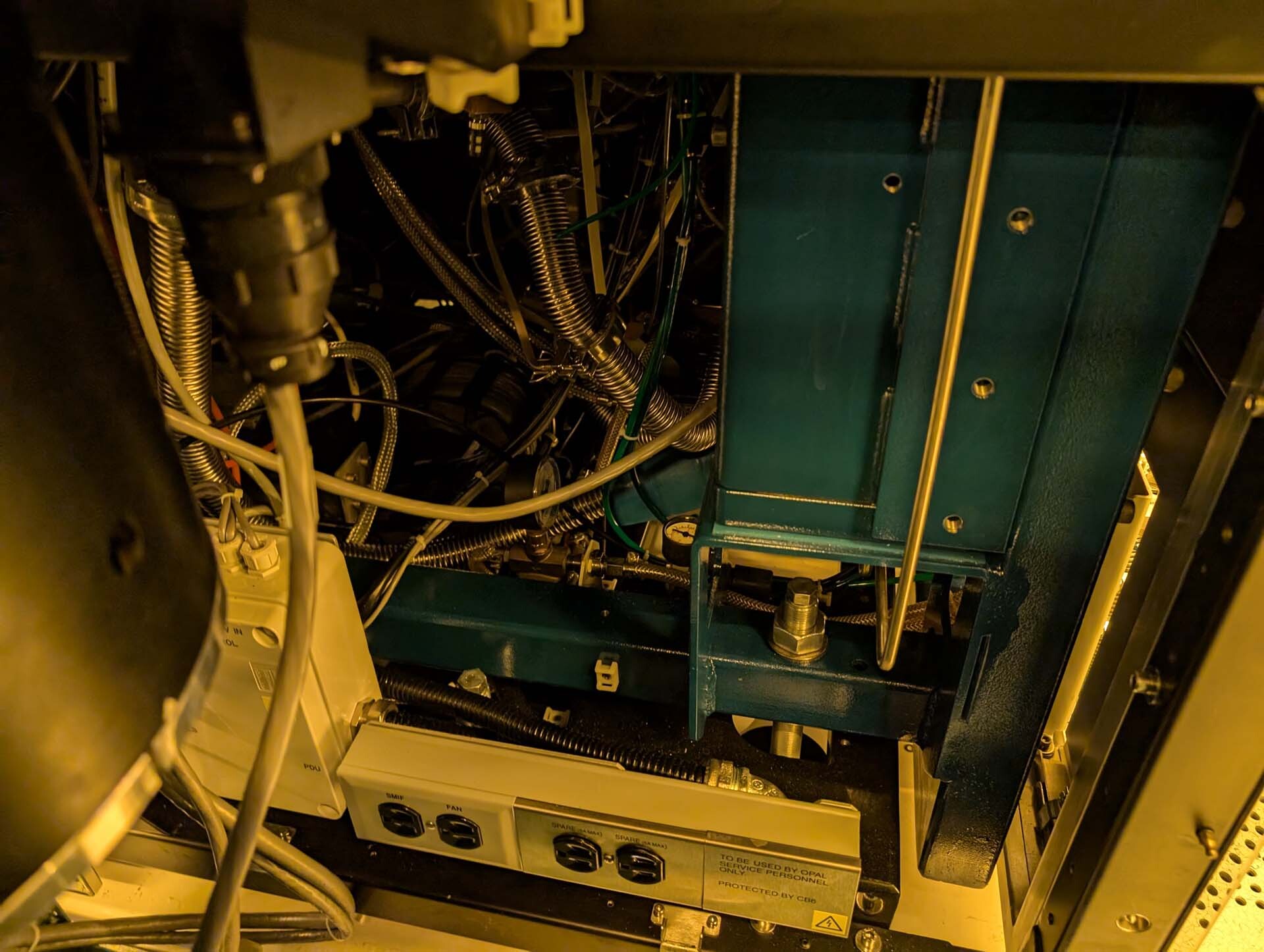
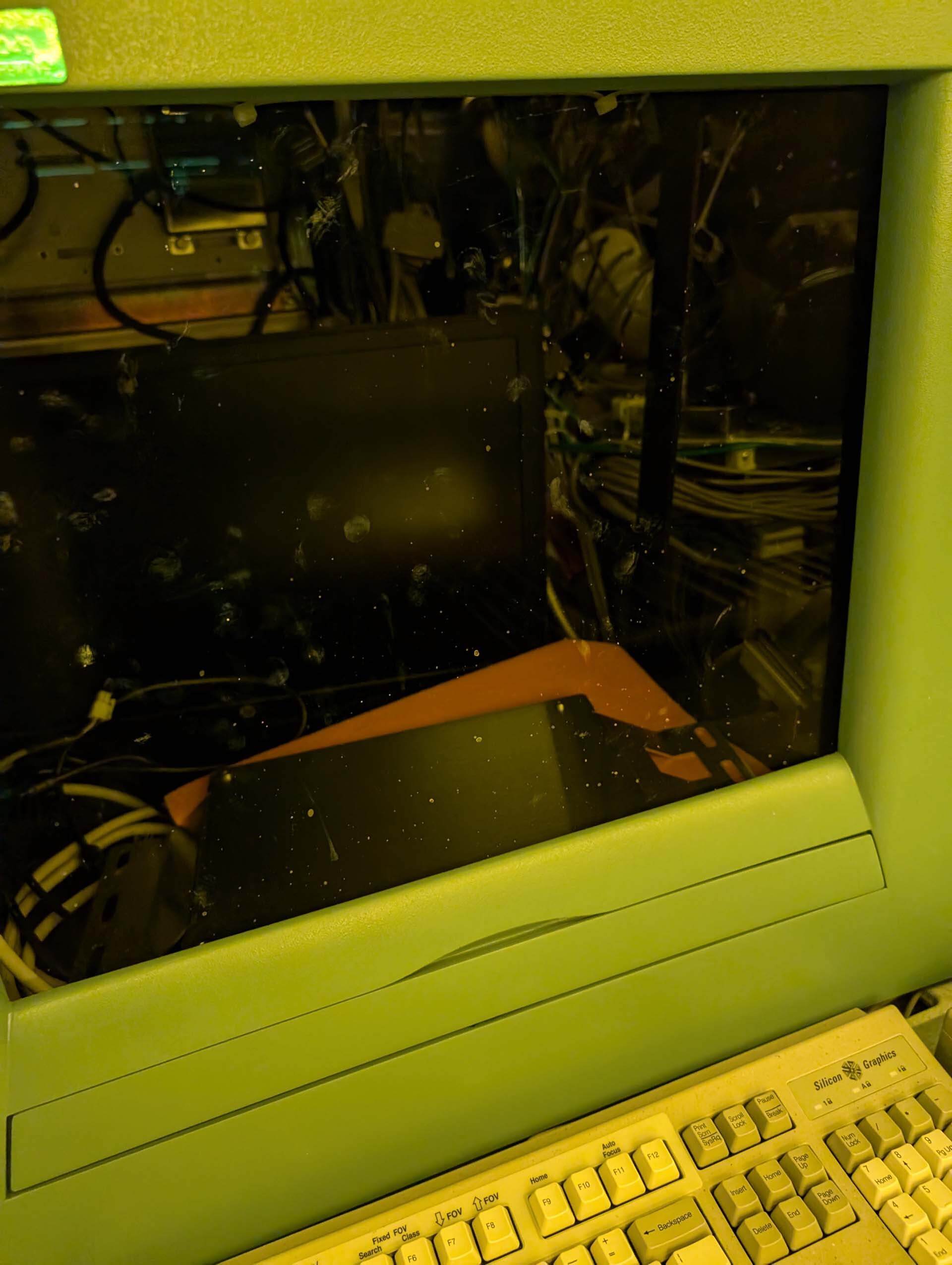
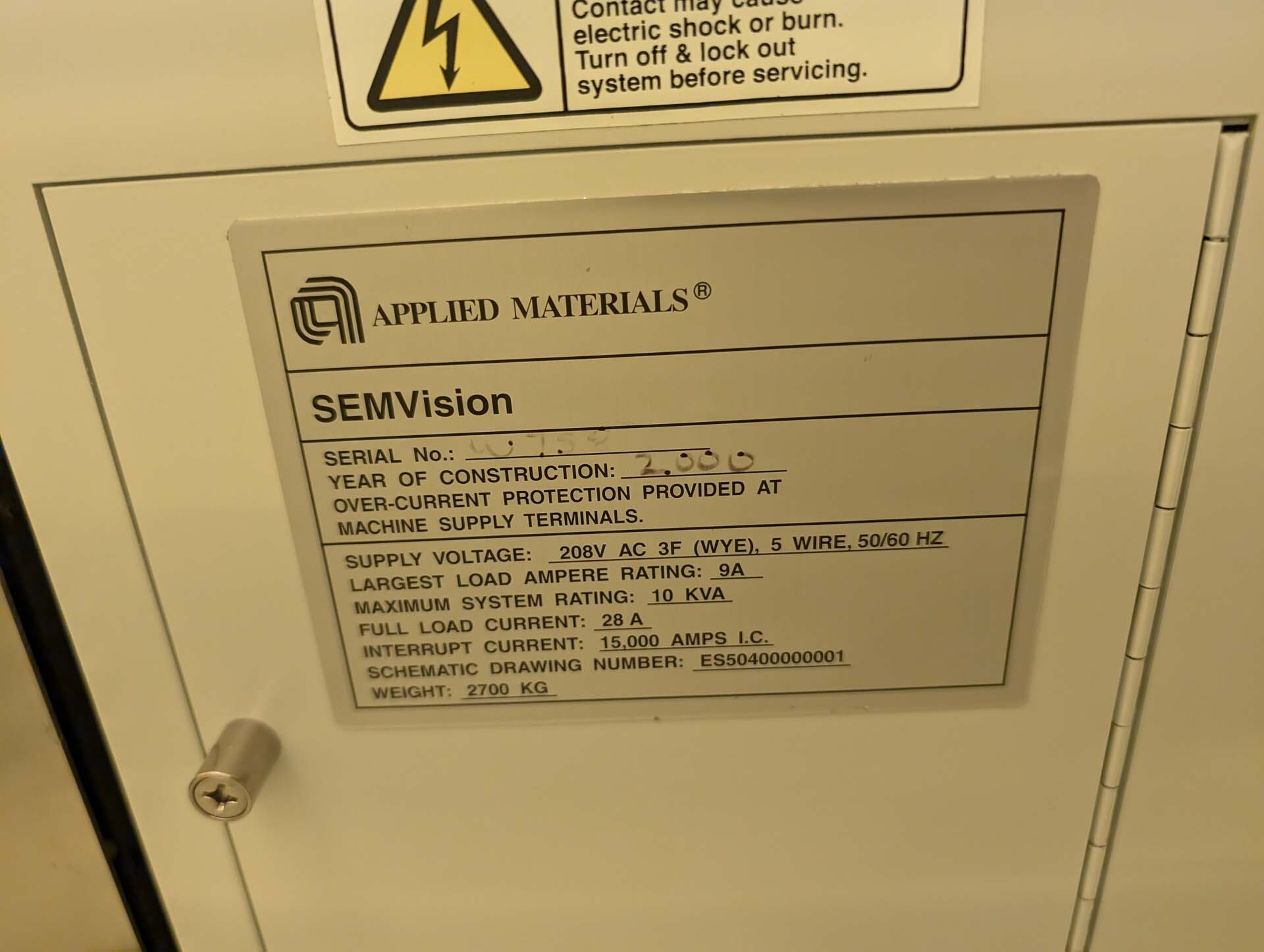
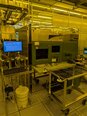
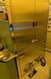
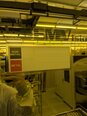
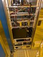
AMAT / APPLIED MATERIALS SemVision is an advanced mask and wafer inspection equipment used for the fabrication of semiconductor wafers. It provides high resolution 2D imaging for a range of substrates and can be used for critical step inspections. The system is based on the scanning electron microscope (SEM) technology and utilizes a range of imaging detectors to achieve high magnifications and resolutions. AMAT SemVision unit features include a high-resolution surface and cross-section observation capability, integrated pattern recognition/inspection, image manipulation, automatic measurement and diagnosis, multi-magnification support, and multiple substrate capabilities. The machine can detect particles, defects, surface roughness, scoreboards, and other wafer integrity issues. The tool includes powerful image analysis and image correlation algorithms for automatic identification and classification of defects. The user interface has been designed for efficient operation and improved user experience. It offers an intuitive environment for feature recognition, defect analysis and evaluation. Additionally, several automated features such as automatic geometry recognition, rapid pattern search and alignment, and automatic pattern recognition help streamline and simplify the workload, enabling faster, more reliable results. As well, the asset offers intuitive graphic navigation and automated screening on a variety of substrate types. The model can be used for inspecting wafer materials such as AsTm, C/SiC, Ge, polyimide and more. Each substrate has its own specific imaging requirements, and the equipment is optimized to accommodate and ensure high levels of accuracy and resolution. The system can also be used for inspecting multi-level masks and other high precision imaging substrates. APPLIED MATERIALS SemVision unit is a powerful tool for performing reliable and accurate inspections and analyses. It offers high resolution imaging capability, automated pattern recognition and image correlation, integrated measurement and diagnosis capabilities, and a user-friendly interface for efficient operation. The machine can be used for a wide range of substrate types, enabling reliable and dependable analysis of a variety of materials.
There are no reviews yet