Used AMAT / APPLIED MATERIALS UVision 200S #293749018 for sale
URL successfully copied!
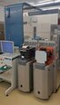
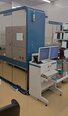

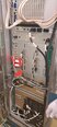

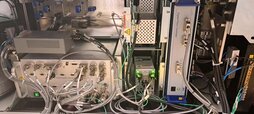


Tap to zoom
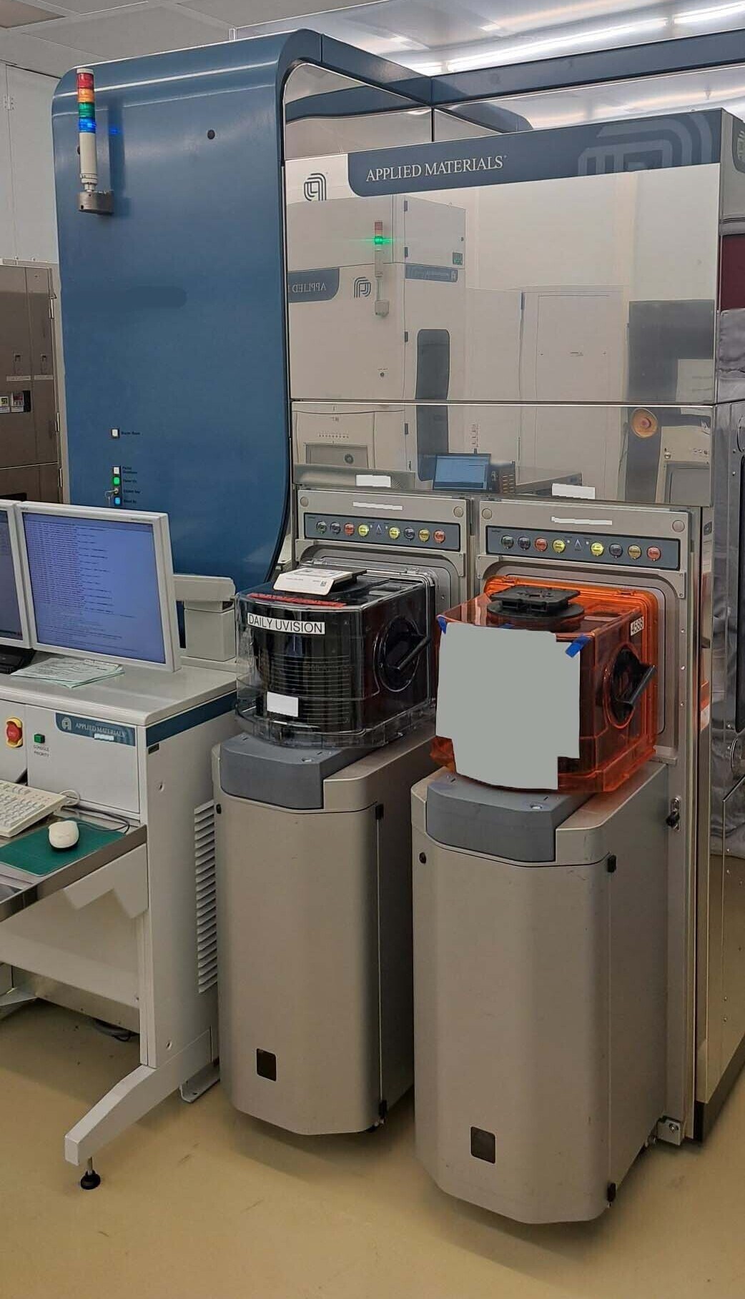

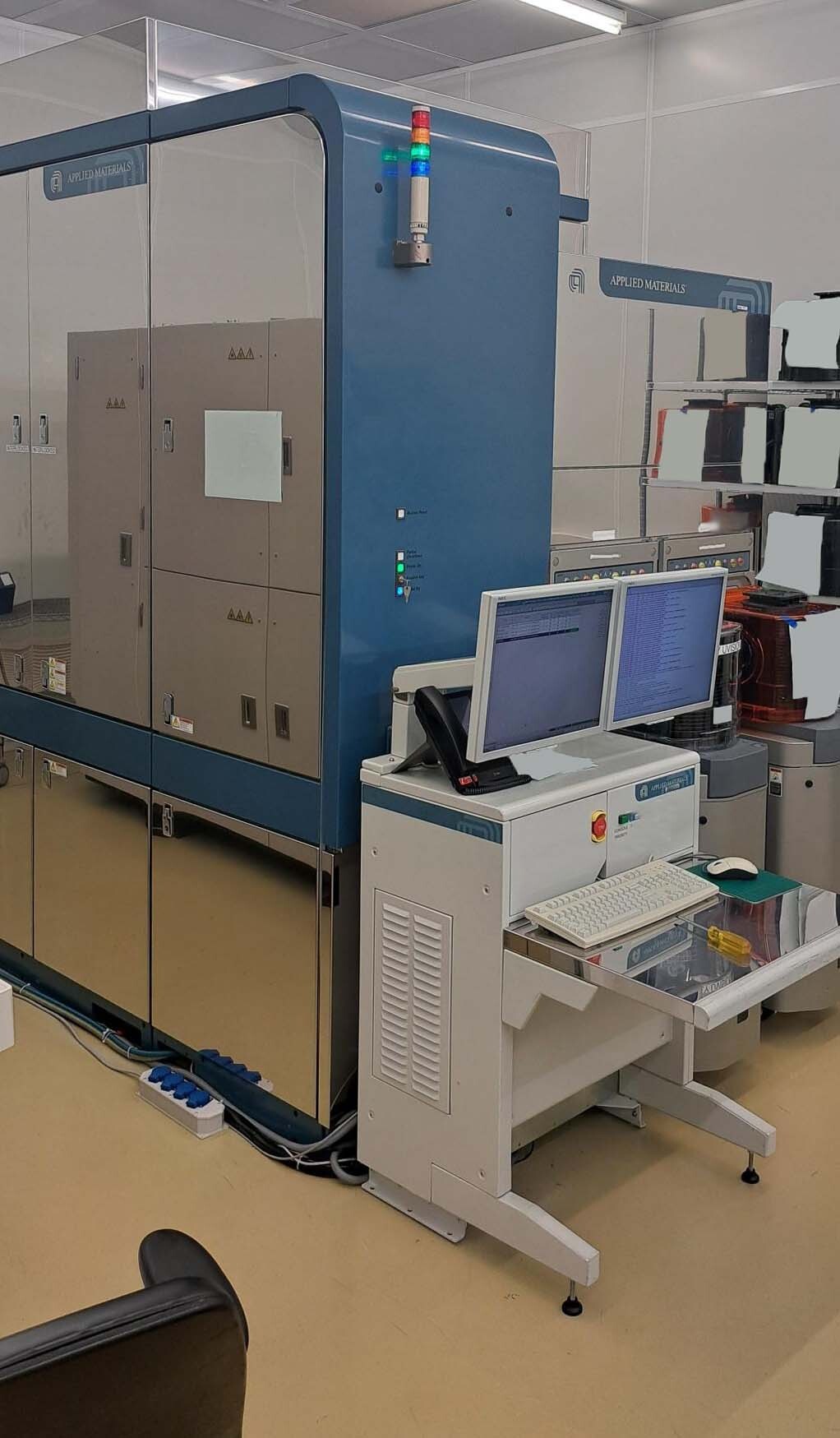
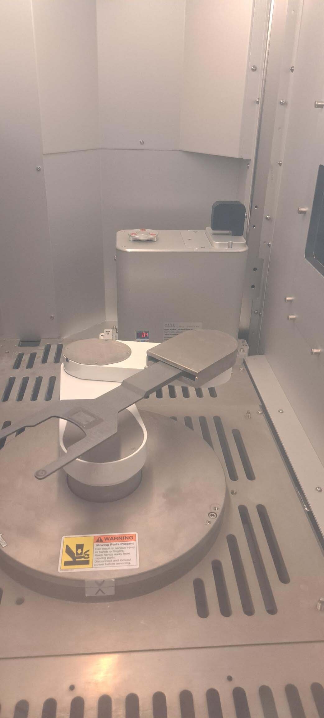
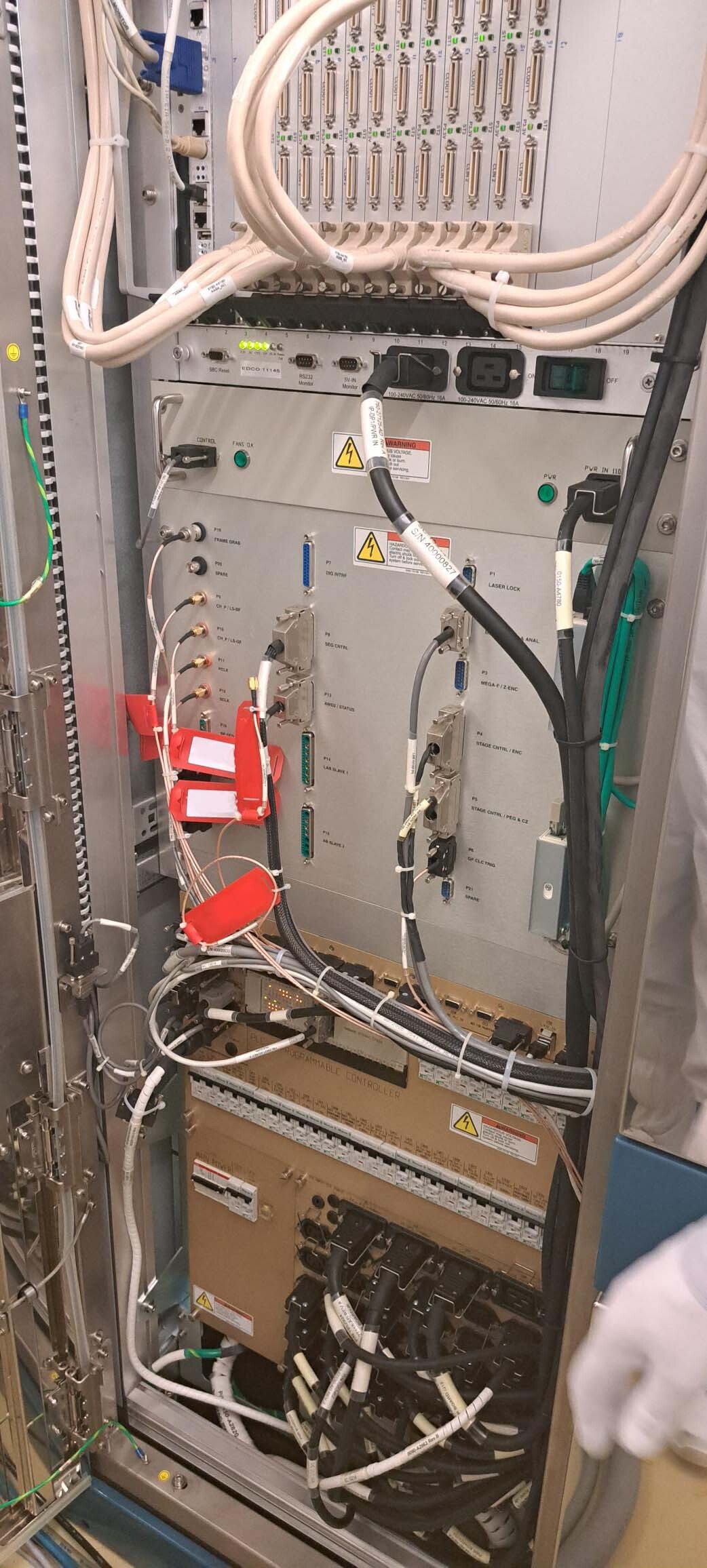
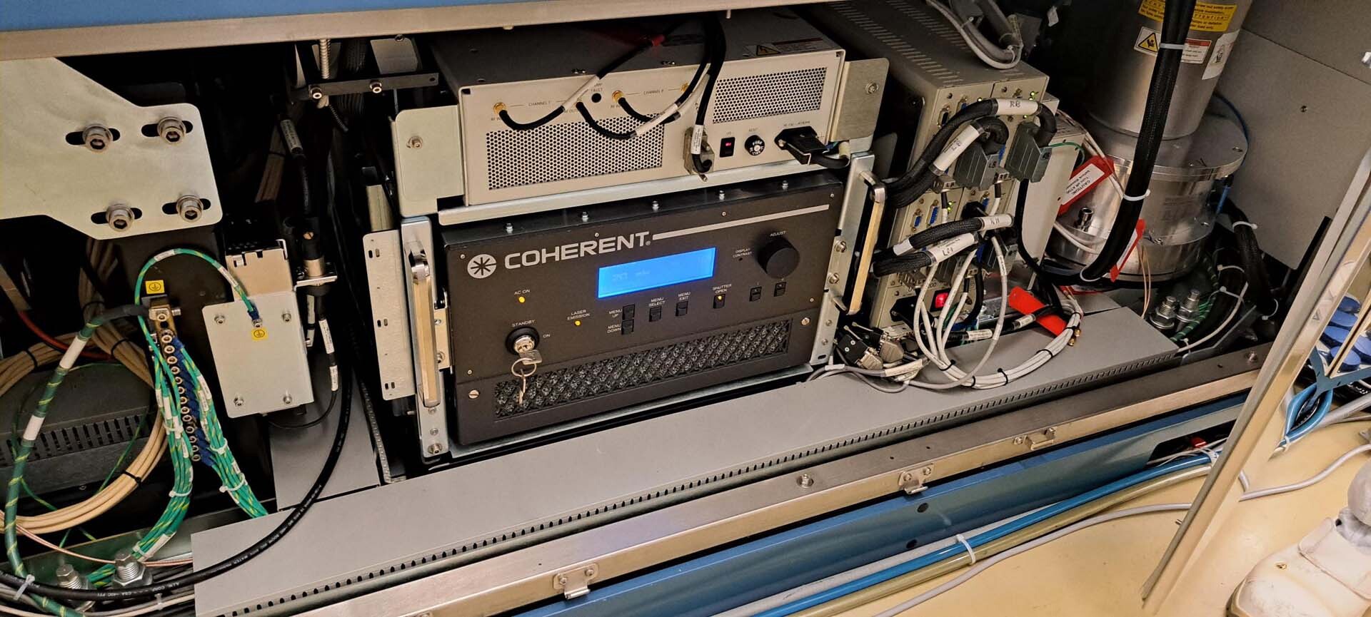
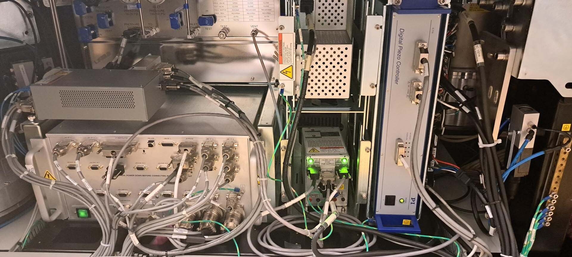
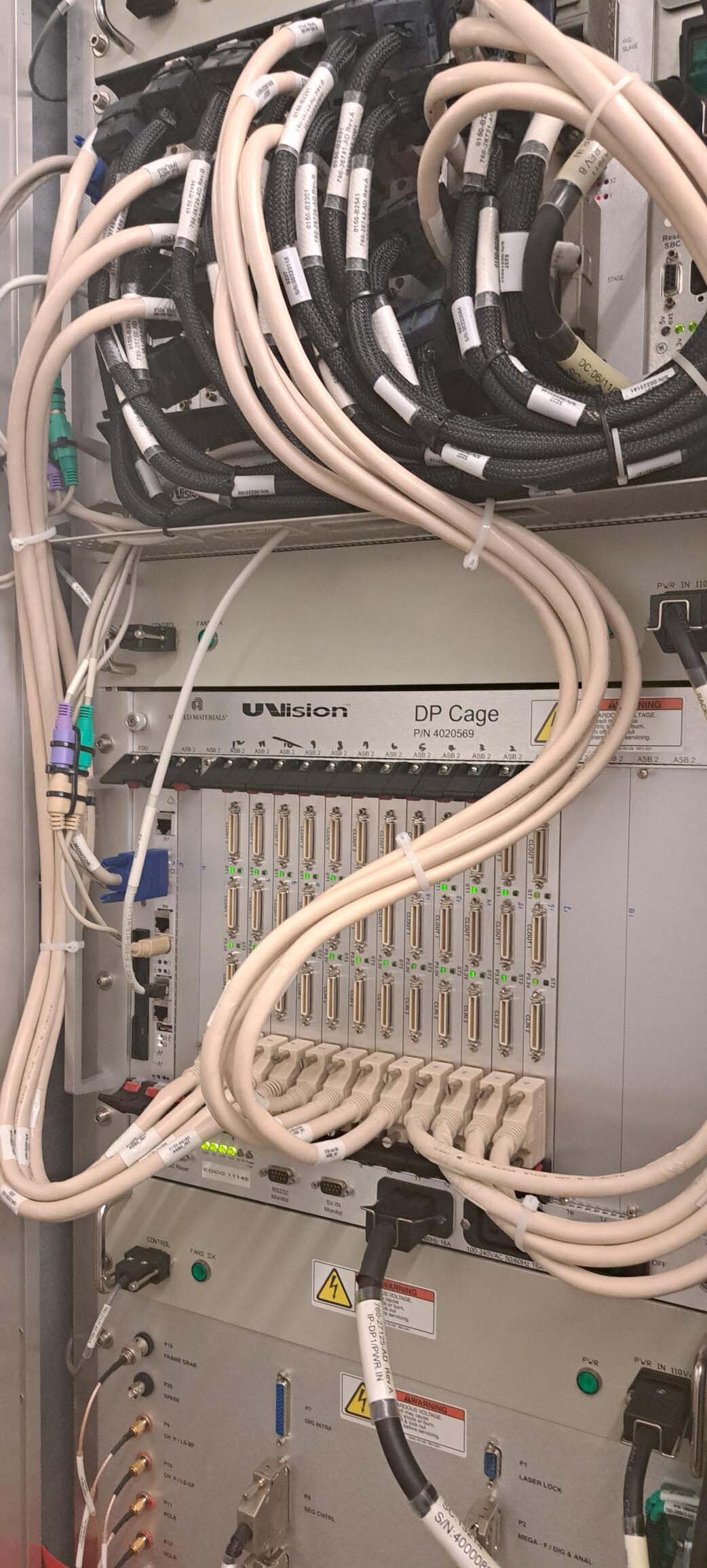
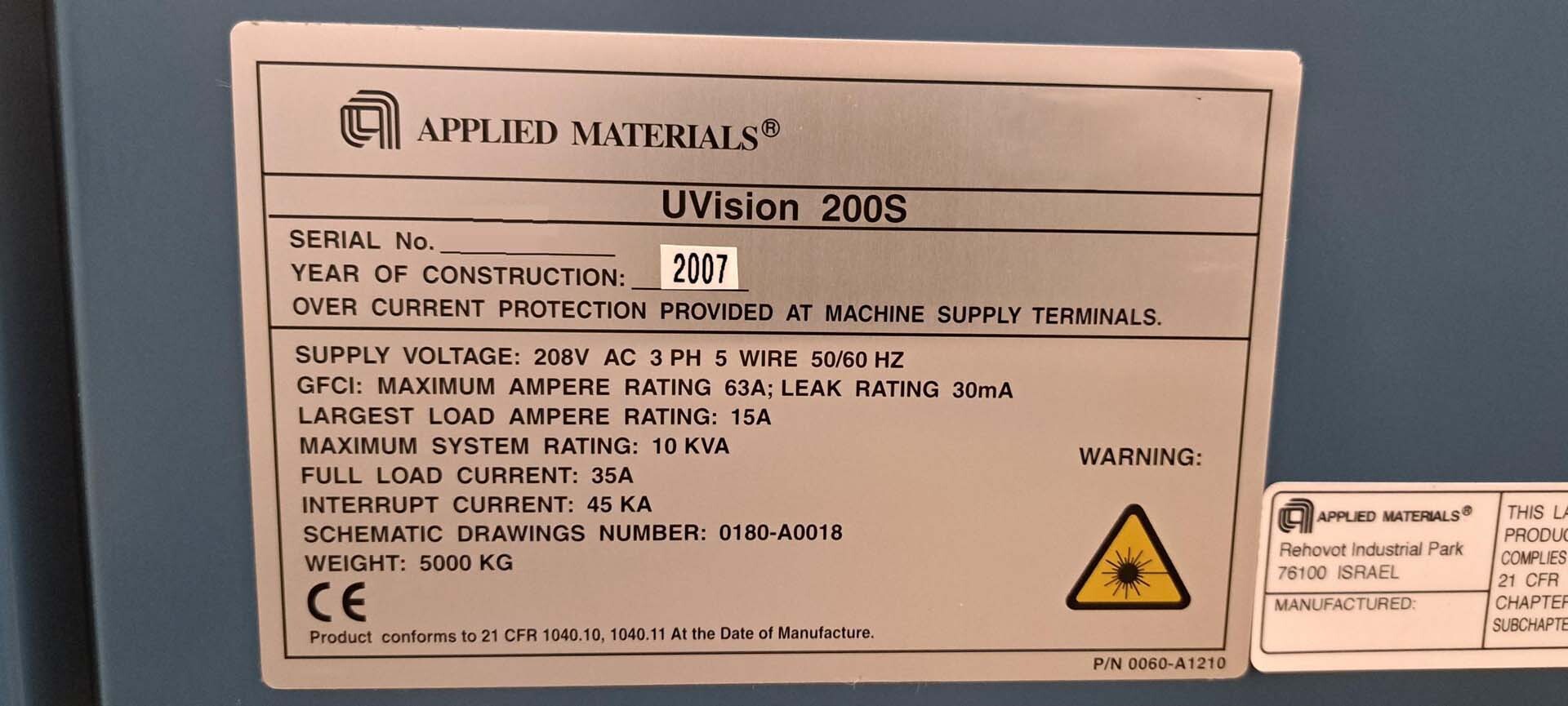
ID: 293749018
Vintage: 2007
Brightfield inspection system
DUV Laser: 266 nm
Polarization controller
Sensitive photomultiplier detector
Brightfield
Scattered light
Greyfield
2007 vintage.
AMAT / APPLIED MATERIALS UVision 200S is a mask and wafer inspection equipment used for semiconductor device manufacturing. The system enables precise defect detection for even the newest lithography technologies, providing detailed images to examine device and mask patterns in real time. AMAT UVision 200S utilizes a state-of-the-art UV laser imaging unit and powerful software algorithms to detect subtle mask and wafer defects quickly and accurately. Combining superior image resolution and advanced algorithms, the machine is designed to detect and differentiate features smaller than 1 micron. This feature detection capability dramatically increases overall defect detection sensitivity. APPLIED MATERIALS UVision 200S is capable of inspecting different types of masks, including reflective, double-patterned, and chrome on glass, as well as both hard and soft reticles. It also offers flexibility in handling various wafer sizes. The tool utilizes a highly sensitive UV laser light source and a high-resolution digital imaging detector to collect and analyze images. Superior optics and the utilization of linear polarizers provide extremely high sensitivity and image contrast for improved defect detection. It is equipped with an integrated automatic focus asset to ensure that the image resolution is maintained. In combination with AMAT powerful inspection tools, the model is able to quickly detect both pattern defects and SAQ defects (systematic or random), such as particles, static electricity, and scratches. This helps to control the entire manufacturing process, ensuring that the result is defect-free. Advanced image processing, classification, and reporting tools are also available for precise, automated analysis. The equipment also provides an output for wafer simulations. Wafer simulations enable designers and engineers to assess the impact of a pattern prior to fab, helping to avoid costly errors and ensure the highest quality part designs. UVision 200S is a modern mask and wafer inspection system that is designed to meet the most demanding semiconductor manufacturing requirements. It is highly sensitive, accurate, and capable of quickly detecting and differentiating features smaller than 1 micron, enabling the highest levels of quality control and product yield.
There are no reviews yet