Used ASM IBE 139H #9150566 for sale
URL successfully copied!
Tap to zoom
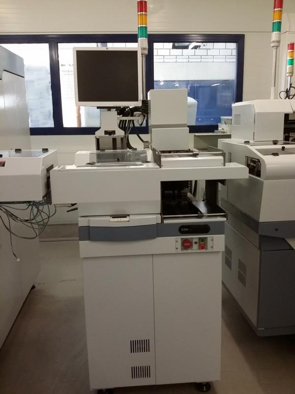

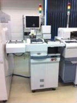

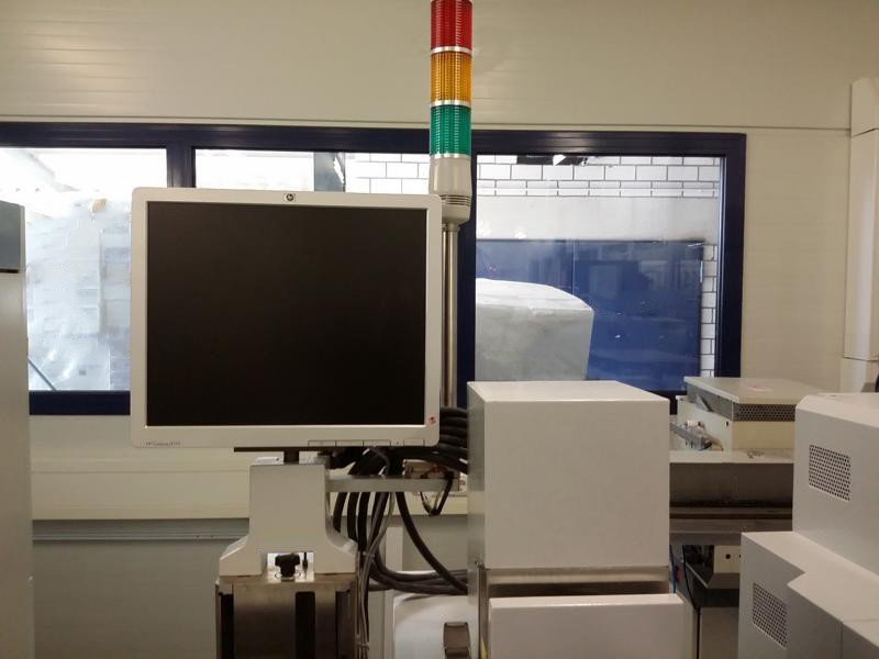

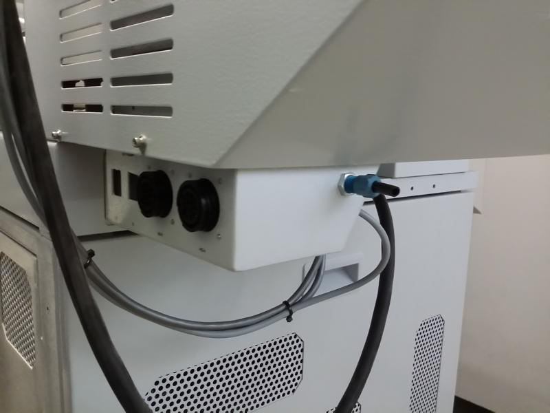

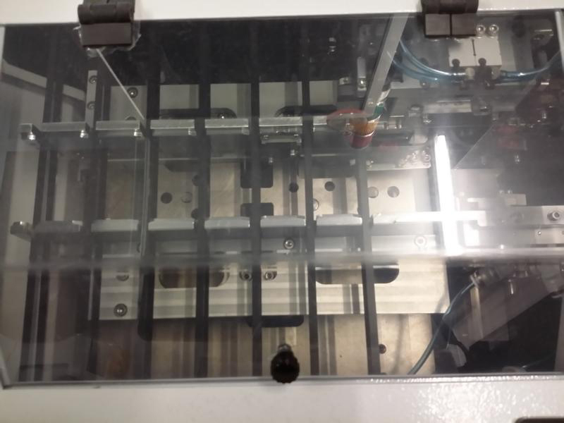

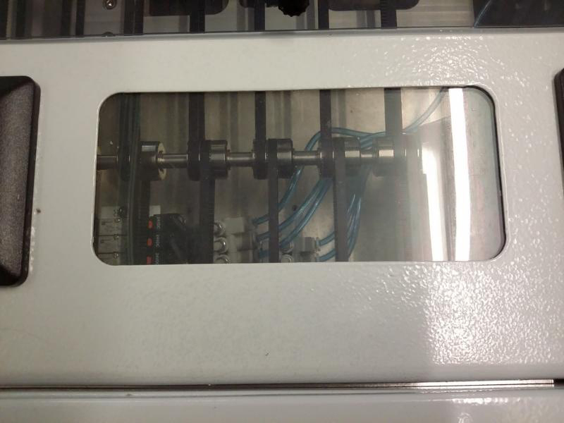


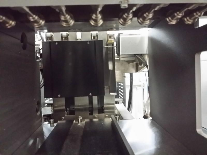

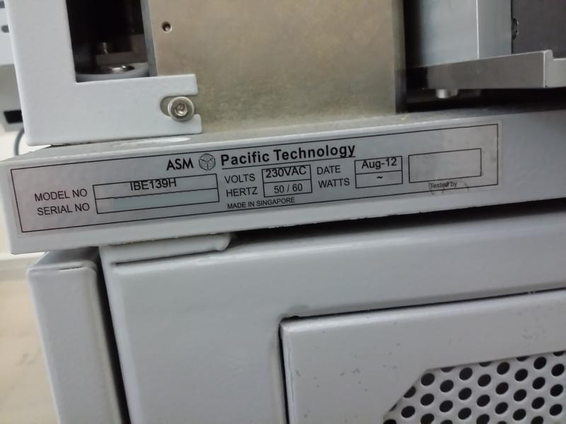

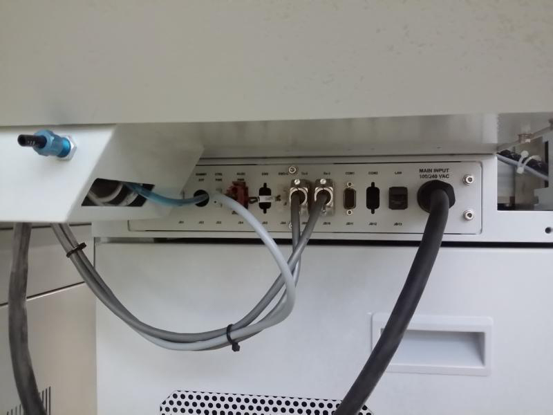

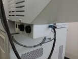
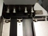
ASM IBE 139H Mask and Wafer Inspection Equipment is an advanced, automated inspection system that provides precise and reliable measurements of semiconductor devices and circuits. It is used for production and research purposes, and provides image-based 3D measurements of multiple features and structures on the device. The unit is engineered with two powerful and high-precision measuring tools in one unit, including a high-resolution vision machine and a complementary air-bearing tool. The high-resolution video asset is used for fast and accurate optical measurements of features in various colors, fine structures, and geometric images. With its resolution of 0.36µm, it can acquire as many as 10,000 separate images of the structure in less than a minute and can provide detailed analysis of both the inner and outer areas of the device. The complementary air-bearing model utilizes air-filtering technology to measure electrical, optical, and mechanical components with high precision. This equipment can accurately measure those features down to 10 microns. The system supports a number of different probing systems, such as air-bearings, needle probes, and force probes. IBE 139H has the capability to measure a variety of mask and wafer sample configurations, including multiple masks, multiple wafers, and varying thicknesses. These samples can range from 0.5mm to 20mm in size. Its advanced optics and probing unit can capture and measure different parts of the structure accurately and rapidly. The software for ASM IBE 139H is also of great value and has a number of features. It includes multi-files support, one-click structure measurement and editing, data analysis and control files, and mask drawing options. The software also provides dynamic reports, user-defined parameters, and error-prevising automation to guarantee accurate measurements. All-in-all, IBE 139H Mask and Wafer Inspection Machine is an advanced and powerful automated inspection tool capable of providing precise, quick, and repeatable measurements of multiple features and structures on semiconductor devices and circuits. It is well equipped with a high-resolution imaging asset and a complementary air-bearing model, making it suitable for production and research purposes. Its user-friendly software makes it easy to use and makes the data analysis accurate and reliable.
There are no reviews yet


