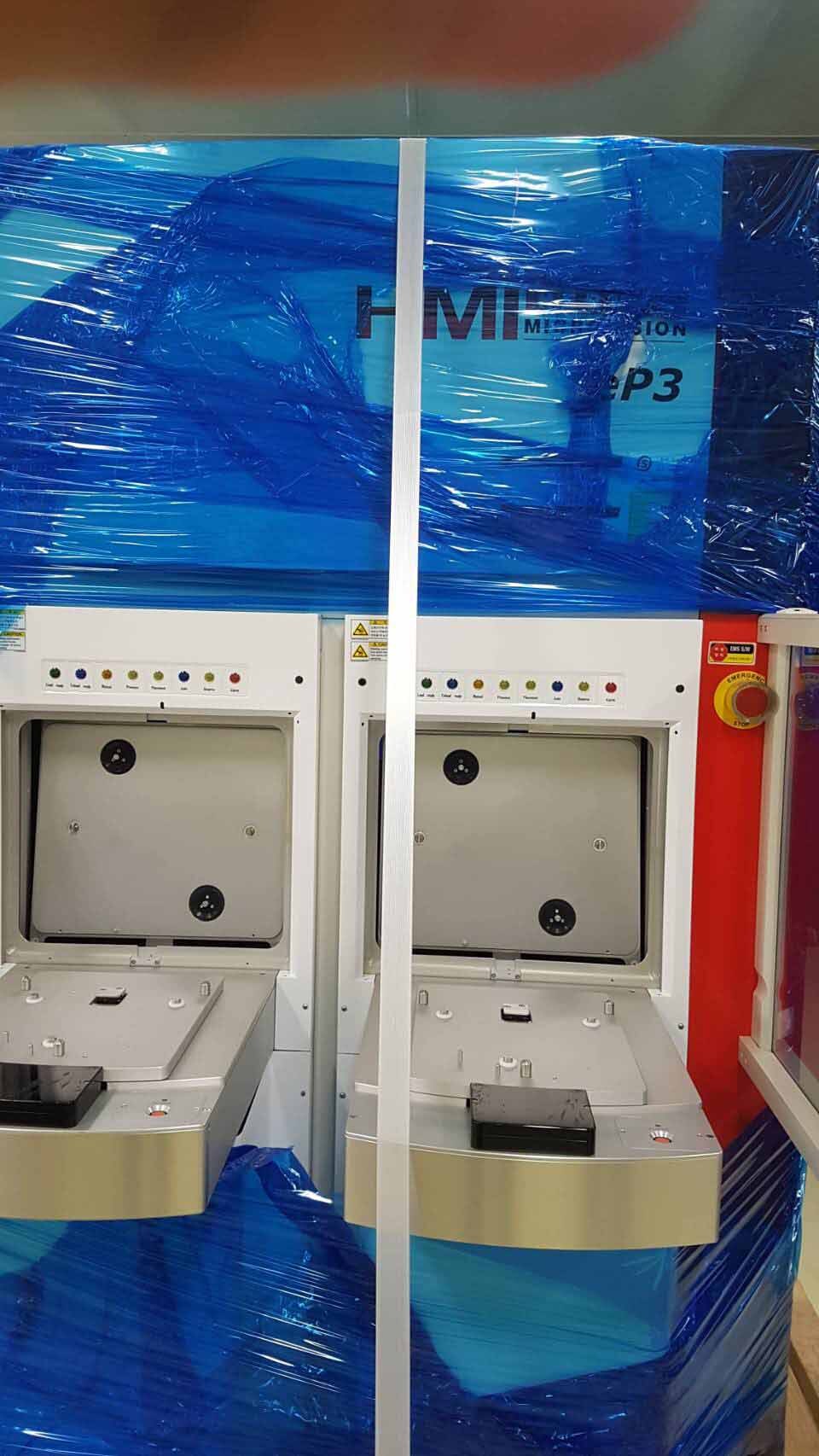
Used ASML / HMI EP3 #293605104 for sale
It looks like this item has already been sold. Check similar products below or contact us and our experienced team will find it for you.
Tap to zoom


Sold
ASML / HMI EP3 is an automated mask and wafer inspection equipment designed to identify, measure and correct defects on individual masks or wafers used in semiconductor lithography. This system combines scanning electron microscope (SEM) imaging with advanced pattern fidelity algorithms and defect detection technology to produce automated assessment of pattern features and performance. HMI EP3 unit features a 200kV electron beam generator, with connected secondary electron and backscatter detectors. It is capable of collecting images at resolutions up to 2nm/pixel and has a field of view from 0.5 up to 4 mm. It also includes an ensemble of software solutions to extend the imaging capabilities of the machine, allowing for measurement of critical dimensions, pattern geometries, pitch values and for quantitative analysis of mask and wafer images. These software tools allow for precise defect quantification and identification including the ability to distinguish defects from background features. ASML EP3 tool also features three-dimensional features metrology capabilities, allowing for quick and accurate dimensional measurements with a resolution down to 50 nm. This is done using multiple views to reconstruct separate images of complex three-dimensional features, allowing customers to measure their wafer stack-up from a single image capture. EP3 asset includes a variety of methods for identifying, quantifying and correcting defects. These methods include automated pattern recognition algorithms for defect identification and for visualizing differences between expected and actual patterns. This model also offers tools for physics-based simulation, allowing customers to understand their process flow and optimize for improved product performance. Lastly, ASML / HMI EP3 offers tools for analyzing mask and wafer images and for making corrections to improve their performance. This includes direct-write technologies for mask and wafer repair, as well as mask and wafer editing software to modify images and patterns. HMI EP3 offers an integrated approach to defect analysis and wafer/mask correction, helping customers to reduce cost and cycle time while maintaining or improving performance.
There are no reviews yet