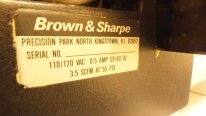
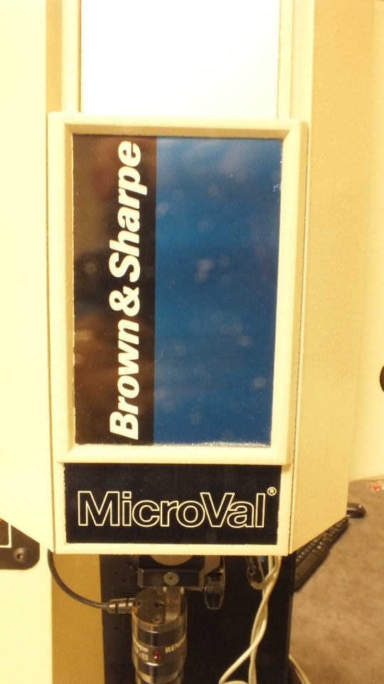
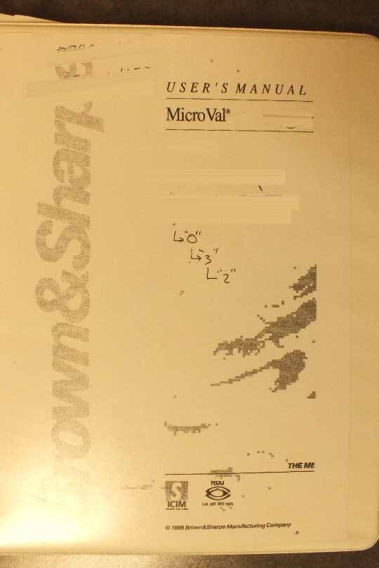
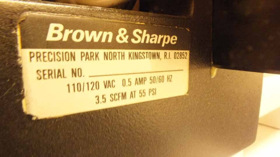
Used BROWN & SHARPE MicroVal 343 #9140610 for sale
URL successfully copied!
Tap to zoom
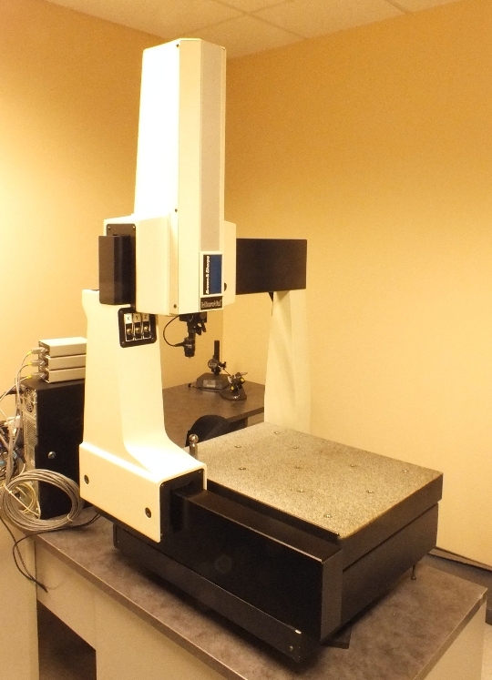

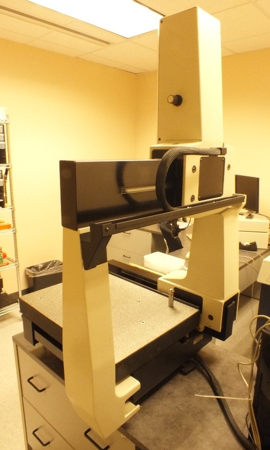








ID: 9140610
Co-ordinate measuring machine (CMM)
Table-top, Manual
NIKON CMM Manager
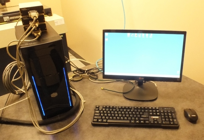
Includes:
Computer
Software
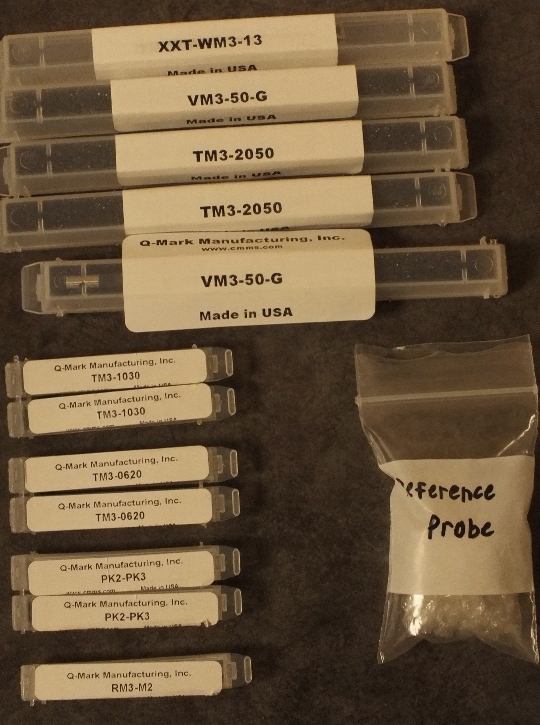
Probes.
BROWN & SHARPE MicroVal 343 Mask & Wafer Inspection Equipment is a comprehensive solution for precision inspection, validation, and analysis of complex semiconductor components. This inspection system utilizes advanced photo-lithographic techniques to deliver accurate two-dimensional and three-dimensional images of tiny features with high sensitivity. MicroVal 343 unit is capable of inspecting both mask and wafer samples of various complex geometries with resolutions of up to 0.25um. The machine's optical imaging tool consists of a high-resolution panoramic CCD camera and a precision LED light source. This ensures that all features, including photoresist patterns, feature profiles, and cavities can all be measured with high accuracy. The asset's software allows the user to capture images which can be analyzed in a variety of ways. For example, the software can detect and identify patterns, while also providing accurate measurements of any given feature on the sample. Additionally, software tools such as edge detection, OCR, and comparison features enable the user to compare different wafers for discrepancies in their structures and features. The model also features automatic alignment mode which ensures all samples are tested accurately and stably, and even provides the ability to resize and rotate the sample image in order to be properly confocal to the optical equipment. Additionally, BROWN & SHARPE MicroVal 343 system has the ability to detect features up to 200um in size, and with its multiple light source configuration, it can examine features in both reflection and transmission modes. Overall, MicroVal 343 Mask & Wafer Inspection unit offers customers a precise and reliable tool for inspecting, validating, and analyzing complex semiconductor components. By utilizing advanced photo-lithographic techniques to deliver accurate two-dimensional and three-dimensional images of tiny features with high sensitivity, this machine performed a valuable service in the semiconductor industry.
There are no reviews yet


