Used CARL ZEISS AIMS #293777435 for sale
URL successfully copied!

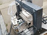
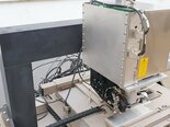
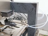
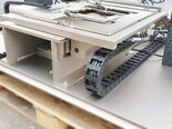

Tap to zoom
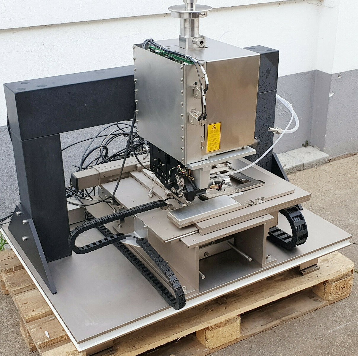

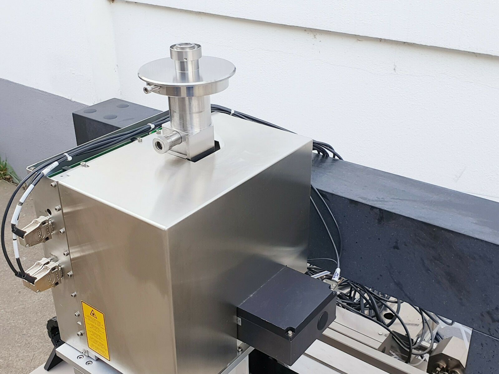
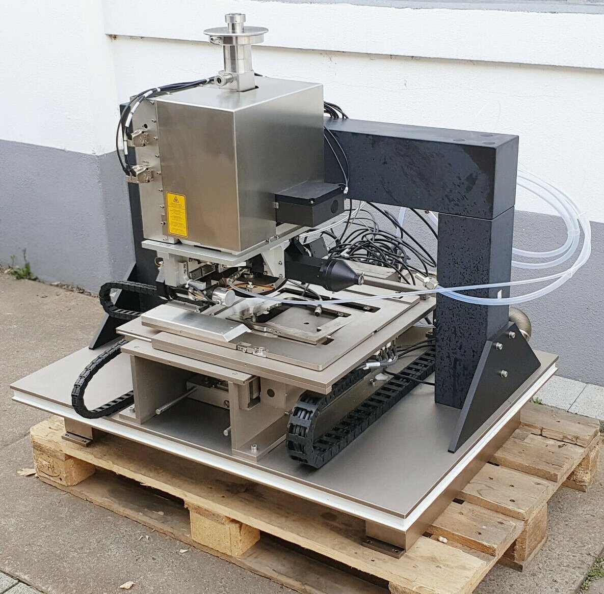
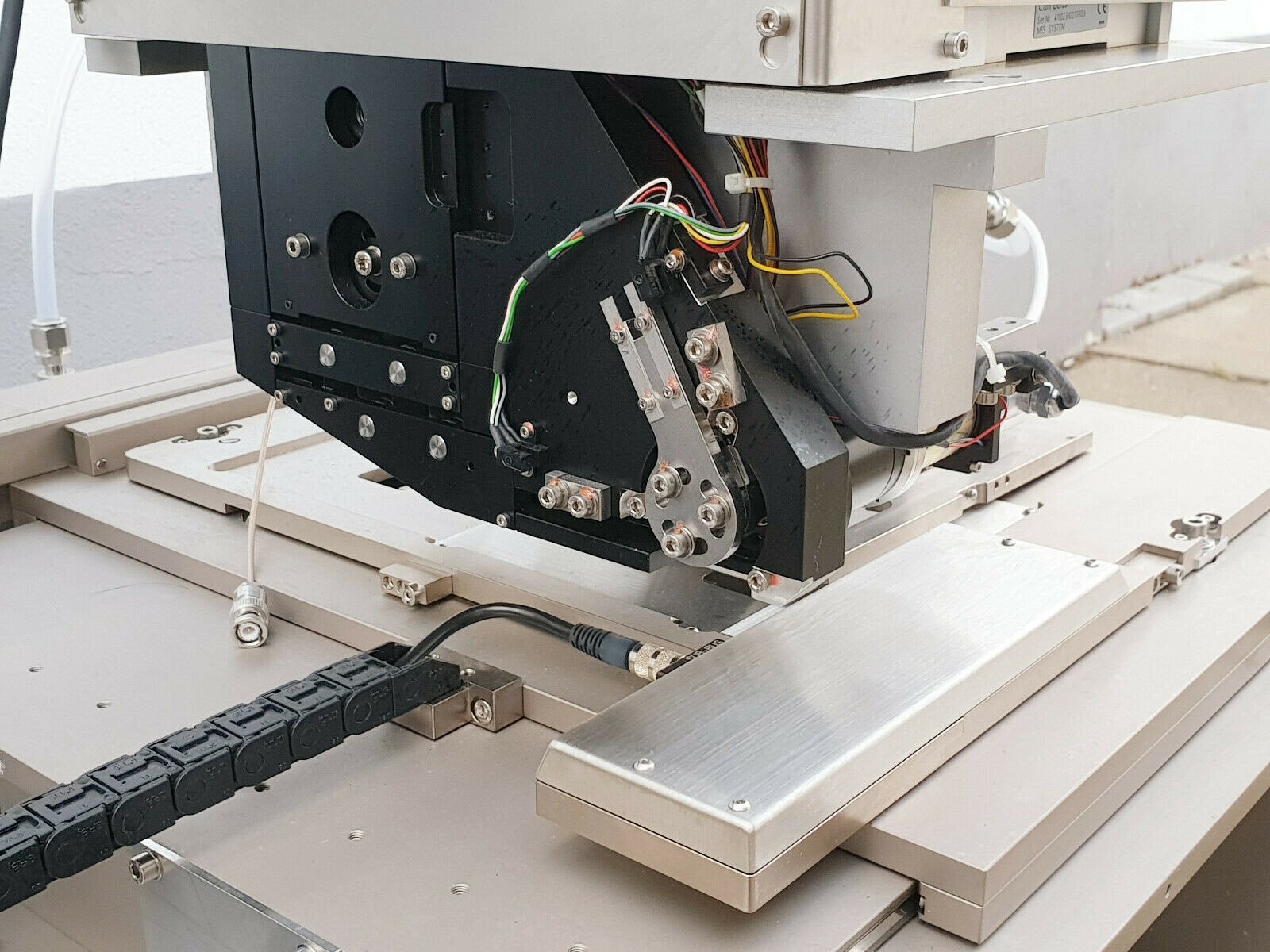
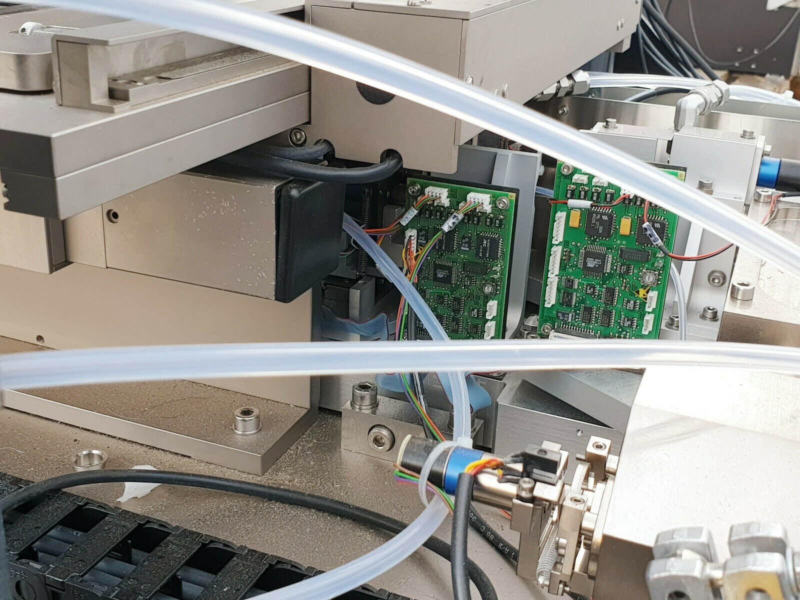
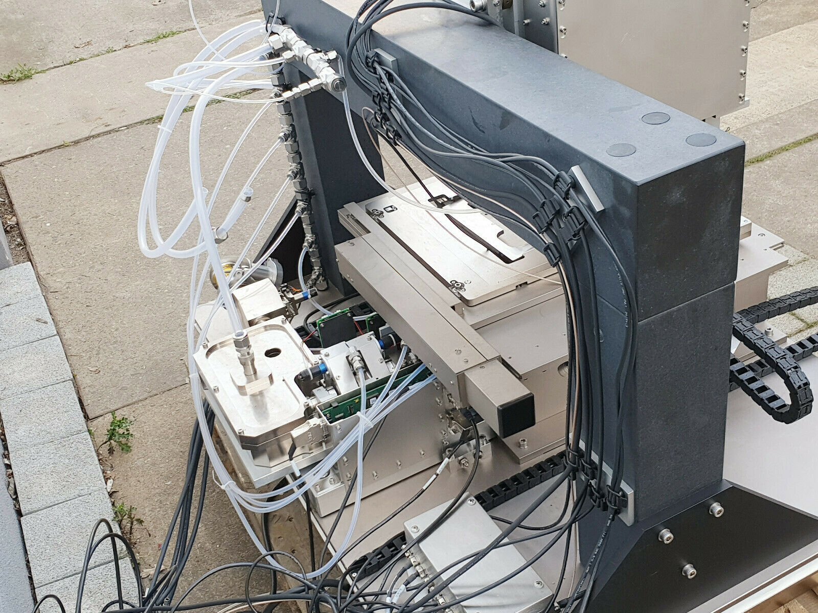
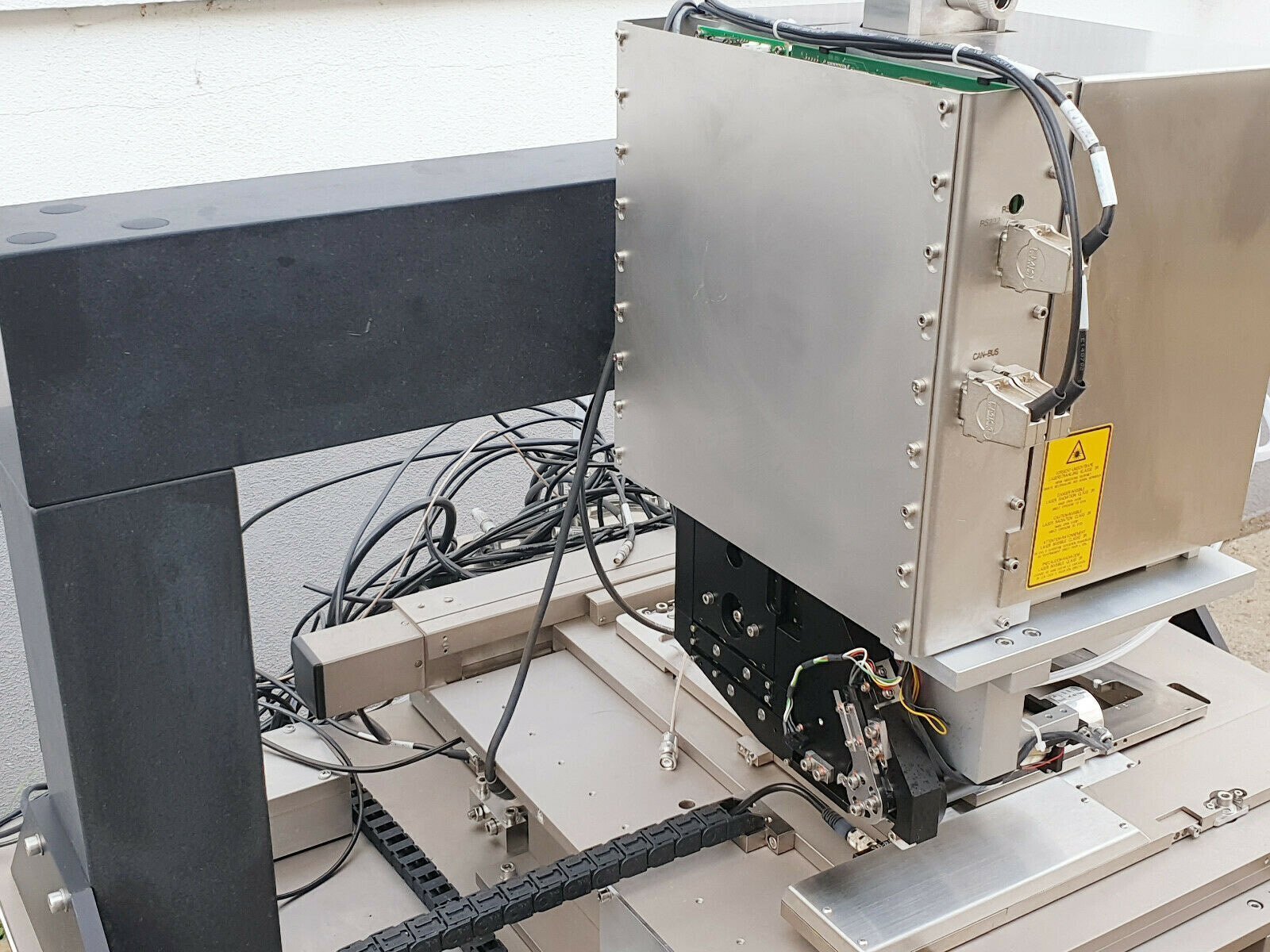
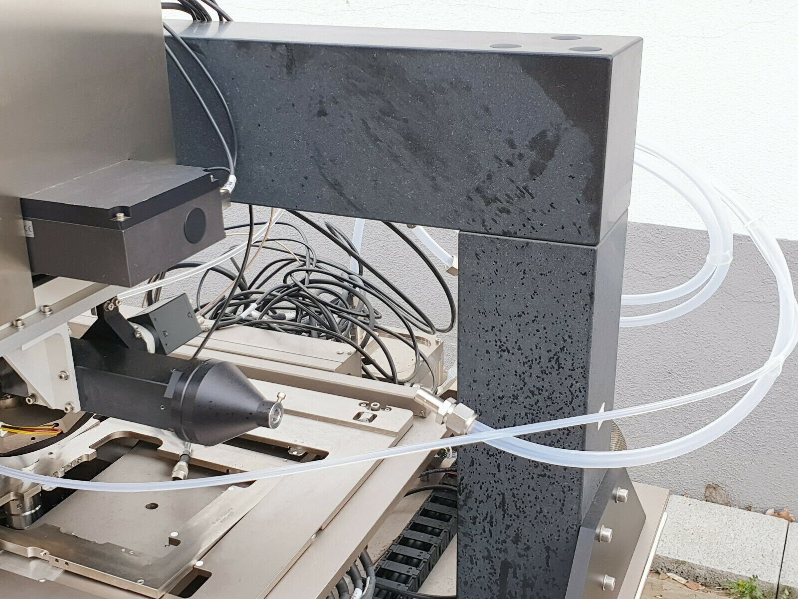
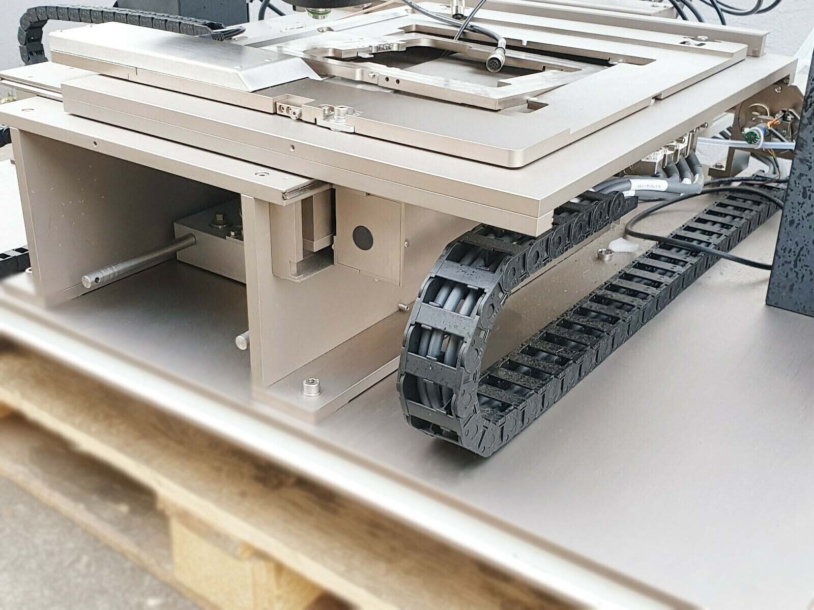
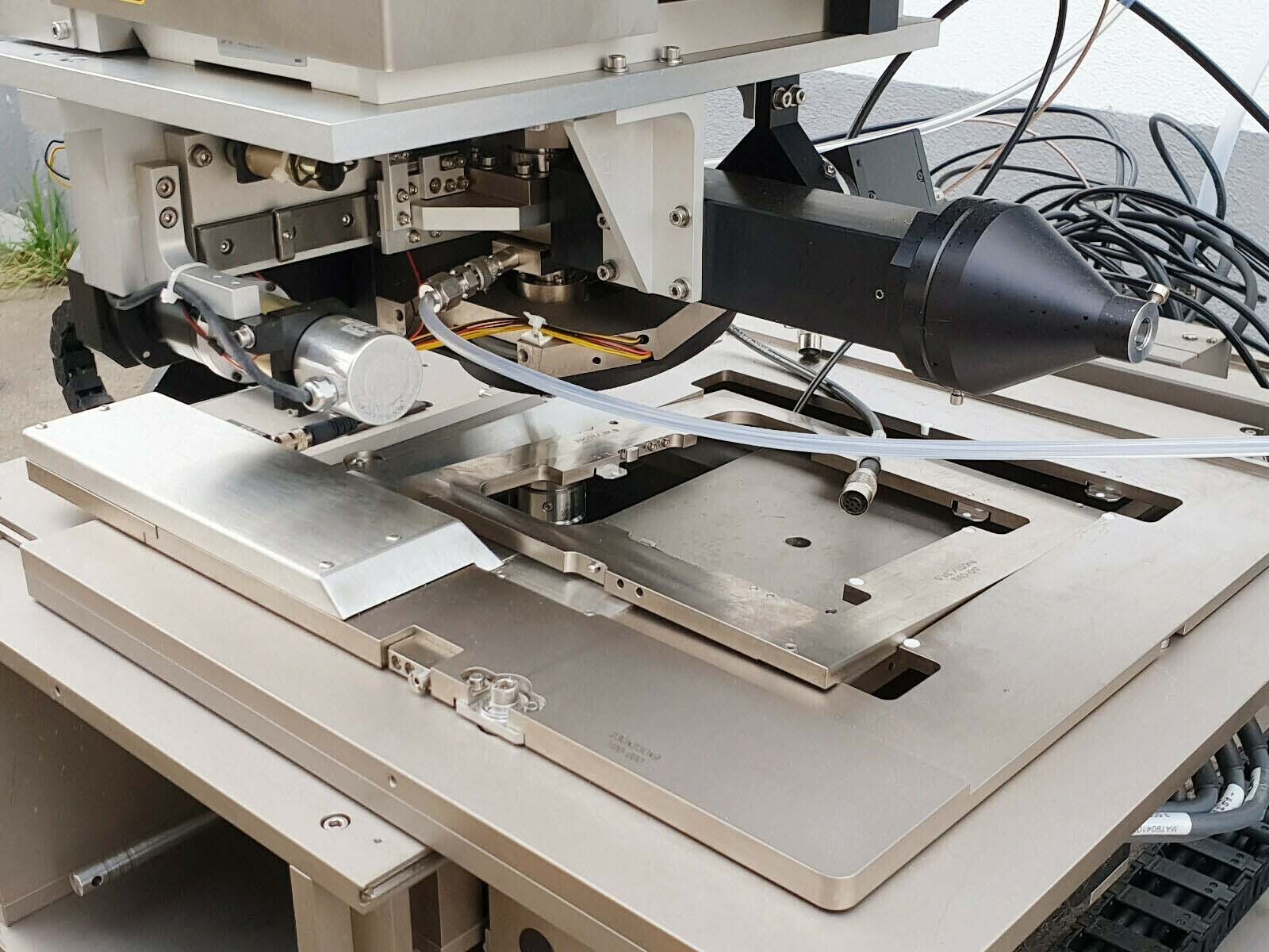
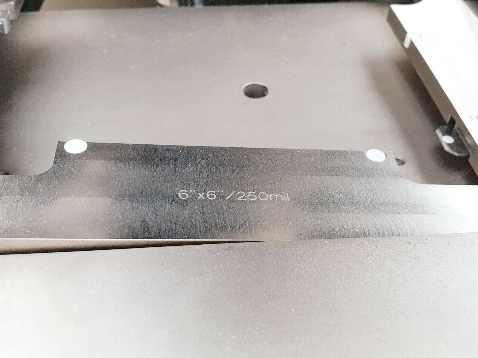
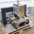
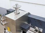
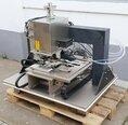
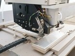
CARL ZEISS AIMS (Advanced Imaging Measurement Equipment) is a highly advanced mask and wafer inspection system developed by CARL ZEISS Semiconductor Manufacturing Technology (SMT). This unit is designed to provide high-precision imaging and measurement capabilities for the semiconductor industry, ensuring the quality and reliability of photomasks and wafers used in semiconductor fabrication processes. The primary function of AIMS is to perform critical inspections of photomasks and wafers used in the manufacturing of integrated circuits (ICs) and other semiconductor devices. These inspections are necessary to detect and analyze defects, such as particles, pattern deviations, and other imperfections that can affect the performance and yield of the final semiconductor products. CARL ZEISS AIMS utilizes advanced imaging technologies, including high-resolution optics, sophisticated algorithms, and precision mechanical systems, to capture detailed images of the surfaces of photomasks and wafers. These images are then analyzed and processed to identify and characterize defects with high accuracy and reliability. One of the key features of AIMS is its ability to perform both aerial imaging and optical metrology measurements on photomasks and wafers. Aerial imaging enables the machine to capture images of the patterns on the mask or wafer without physical contact, providing a non-destructive and highly accurate inspection method. Optical metrology, on the other hand, allows for precise measurements of critical dimensions and features on the mask or wafer, ensuring compliance with design specifications. In addition to defect detection and measurement, CARL ZEISS AIMS can also perform advanced analyses, such as pattern matching, overlay measurements, and process control monitoring. These capabilities are essential for ensuring the quality and consistency of semiconductor manufacturing processes, helping to minimize defects and improve yield rates. The tool is equipped with a variety of specialized modules and accessories, including advanced illumination sources, high-speed cameras, and automated handling systems, to support different inspection requirements and applications. It also features a user-friendly interface and software tools for data visualization, analysis, and reporting, making it easy for operators to set up and perform inspections efficiently. Overall, AIMS represents a cutting-edge solution for mask and wafer inspection in the semiconductor industry, offering unmatched precision, reliability, and performance. By leveraging advanced imaging and measurement technologies, this asset helps semiconductor manufacturers ensure the quality and integrity of their products, ultimately contributing to the advancement of technology and innovation in the semiconductor industry.
There are no reviews yet